For curiosity sake... i was talking about the different CELL pad layouts before, but today i made a comparison that is going to clarify some of the speculations
The point is... there are up to 4 CELL pad layouts, but 3 of them matches in the 41x41 number of pads in the peripheral (differs in the missing pads at the center "hole" though)... so we was wondering if soldering a different CELL revision in the pad layout of other CELL revision could affect
ONLY the pads at the center
https://www.psdevwiki.com/ps3/CELL_BE#Alternative_listing
CELL 90nm (41x41)-(19x19)-84 = 1681-361-84 = 1236 pads layout
CELL 65nm (41x41)-(15x17)-84 = 1681-255-84 = 1342 pads layout
CELL 45nm (41x41)-(17x17)-84 = 1681-289-84 = 1308 pads layout
CELL 45nm (42x42)-(22x18)-9 = 1764-396-9 = 1359 pads layout
In wiki there is an image of the CELL 90nm pad layout, and the pinout, from the COK-001 or COK-002 manuals
https://www.psdevwiki.com/ps3/CXD2964GB
And i just started a page with the pinout of the CELL 65nm, from the SEM-001 manual, and i made this image following the same rotation for comparison purposes
https://www.psdevwiki.com/ps3/CXD2981GB
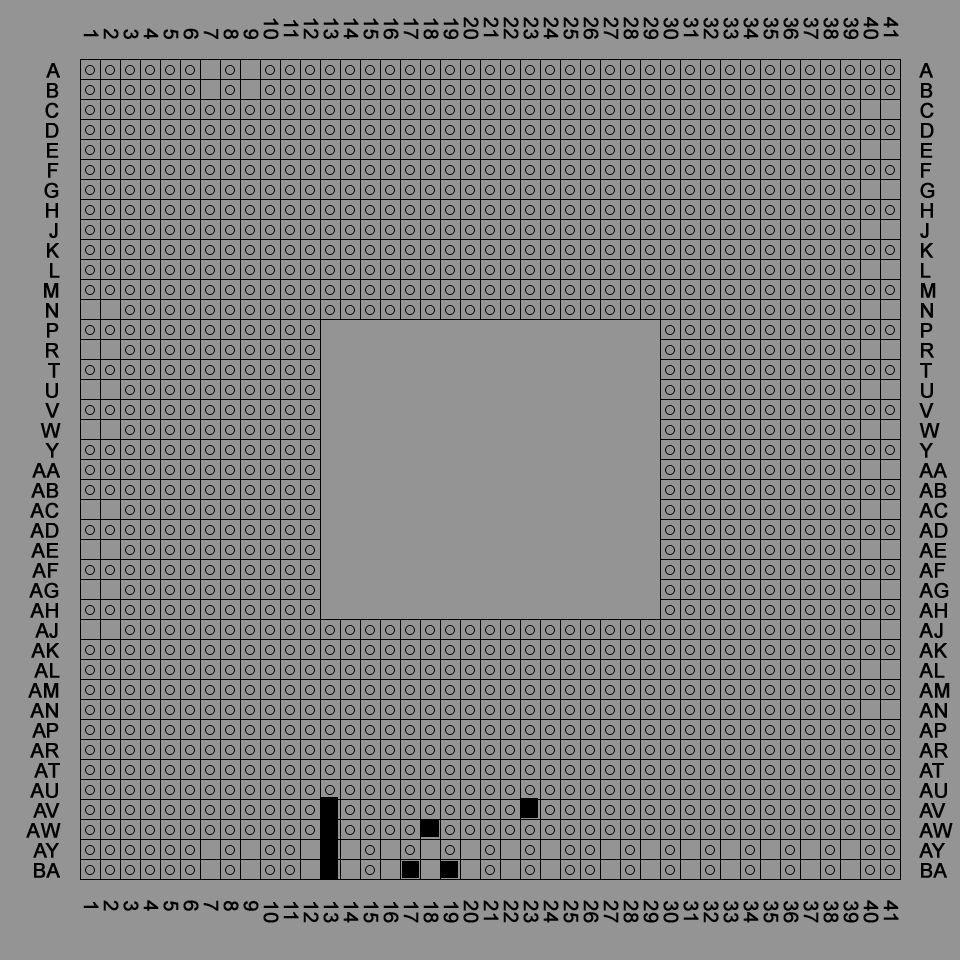
Long story short... i marked the CELL pads dedicated to syscon connections (8 in total, included the SPI channel) and the location doesnt matches
In other words... if we solder a 65nm CELL in the pad layout of a 90nm CELL this 8 pads dedicated to syscon are not going to be correctly connected, to have a beter understanding of how many pads has been moved it would be needed to continue doing this drawings painting more pads of the 65nm layout in colors to compare them with the 90nm layout, but anyway... by now it seems the only way would be by using some kind of intermediate "CELL adapter" board