PS3 Idea for delid tool that won't scratch the substrate

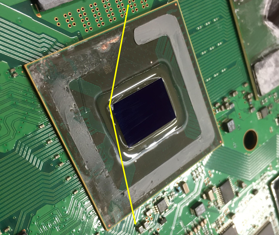
I remembered that razors used to be the original tool used when delidding first became a thing for PS3s, but was quickly abandoned because of how easily it could cut the substrate.

Has anyone tried plastic razors instead? (Like this: https://www.amazon.ca/Scraper-Double-Stickers-Adhesive-Remover/dp/B08BRY8DC8/)

It's already used to prevent scratching sensitive surfaces that a metal razor blade would ruin. So why not use it to delid?
It's an interesting idea and might be useful. I think the thing you'd have to consider for would be what kind of handle of sorts would you use to guide that under the IHS. You'd need some strong, angled just right, and thin enough to get under the IHS and on top of the thermal glue. I wanna say it's like .15 or .015 of a mm or something if I remember correctly. It's a tight friggin space. That's why so many accidents get made.
 
Last edited:
The safest way is always the wire, but the most important thing is the technique. Without learning the proper technique, you won't defeat that silicone on the arena.

While I summon sensei @sandungas, I will leave some examples..

https://www.reddit.com/r/PS3/comments/oilndo/a_warning_about_cutting_wirefishing_line_to_delid/
https://imgur.com/a/7QmTkHg

https://www.reddit.com/r/PS3/comments/tzs1rs/my_first_lousy_delidding_chipped_edge_exposed/
https://preview.redd.it/z2e8u3lpwhs...bp&s=4b884eea370a69ea5d59fcad8e0fc9eb28a8eb99

Both consoles survived btw, barely alive.

Now, sandungas, can you explain me WITAF means that last photo? O.O
 
Now, sandungas, can you explain me WITAF means that last photo? O.O
The silicon is like a mineral (rock), the circuit is "printed" at his bottom, so is only broken if there is a "fracture" that affects the bottom
In the photo it can be seen how the top corner of an edge of the silicon was broken and some "rock shards" was taken appart, but it seems the fracture didnt affected the bottom
In other words... the edges of the rock are a bit damaged but the electronic circuitry is fine, he was lucky :D

And im pretty sure if happened because he was insisting cutting the same corner with the wire too much... lets say he went "too deep" in that corner
2gssrr7uwhs81-copy.jpg


The yellow arrows represents how he was pulling from the wire, it was touching the corner of the DIE, also it can be seen the cord of silicone at the right of the yellow arrows is intact, probably he opened it like a book because he just cutted around 40% of the silicone cord at a side

In my oppinion is a lot better to start by cutting the 4 corners first because are a lot more weak... this should loose a bit the bounding
In other words, after cutting the 4 corners the gap in between IHS and the DIE becomes a bit bigger (few micrometers) so is easyer to continue cutting
 
It seems the guy used the painter knife, which is the tool that I don't recommend, precisly because things like this CAN happen.

"I used oil painter knife #1. But the key is heating up the IHS to be hot enough to soften the glue. I set my hot gun to 200C."

My first fat ever, H, died when I was trying to delid it, I surely cut some traces and later saw one hit at the die, the main reason why I thought it perished, but that pic changes everything.

You know, I think that mineral and later the real chip under of it looks a lot of how screen (tv/cell phone) is "attached" to the flex. Is not soldered, but both are united. If the crystal cracks, forget about those lines, or even the complete screen.

 
There is an old video in youtube (as far i remember made by that TV show named "how it's made") where it can be seen how are build, it was a factory from global foundries or TSCM or something like that
They melts the silicon at huge temperatures and they "drops" it verticall from the cellar, like a giant sausage with chrome color
After that (when the sausage gets cold) they cuts it in slices, like peperoni, lol
Then they starts dropping layers of chemicals in the slice, and "shoots" at it with ligh rays, this process is repeated many times with many different layers of chemicals. Is pretty much like "3D printing" in the rock surface

So... the printed circuit is "outside" of the rock... if the bottom surface of the silicon breaks then the circuit is broken... but all other tiny fractures or shards (not affecting the bottom of the silicon) doesnt damages the circuit

*And the thickness of the peperoni slices i guess is just the thickness they decided is good enought to resists the small mechanical deformations (caused by bending, wrapping, etc...)... but the fact is they could cut that slices of silicon a lot more thinner
The screens of the smartphones are a lot more thinner, half the thickness or a thrid part of a DIE... so the probabilities for a fracture to affect the bottom layer is a lot higher in a smartphone screen
 
Last edited:
Back
Top