RIP-Felix
Senior Member
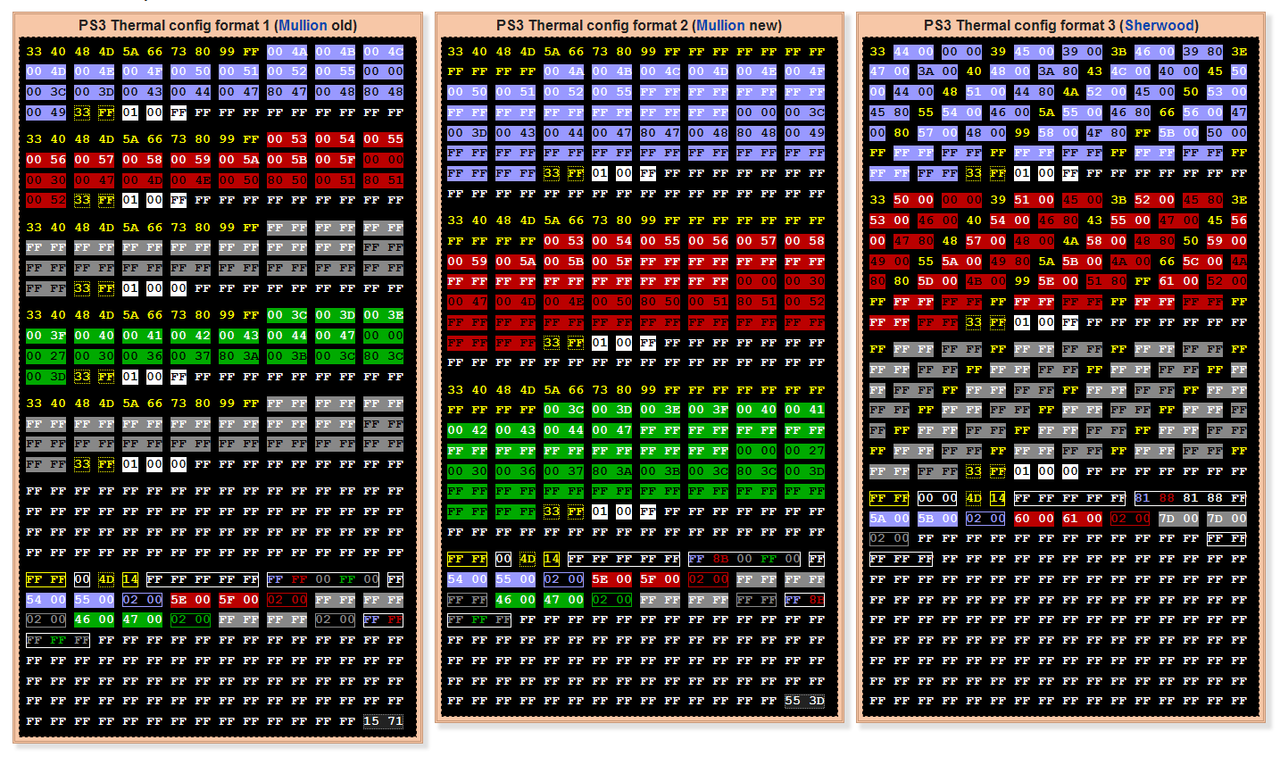
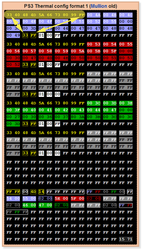
We should get these entered at some point on the wiki now that more of the thermal configs have been dumped.
>$ revision
>$ version
>$ tzone
>$ fantbl get 0
>$ fantbl get 1
>$ tshutdown get 0
>$ tshutdown get 1
>$ eepcsum

")
What happened with that board ?, i hope you still have it and the syscon is alive to run that commandsGood got a scrap dia002, will dump it in few days.
>$ errlog
[SSM] state: 0600 -> 0000
[SSM] Error state is cleared.
(PowerOff State)
[SSM] state: 0000 -> 0101
Bringup Mode #0 (0xFF)
[SSM] ssmCb_OnStartingBePowOn() called.
[SSM] Bringup mode : syspm_stat=00000000/00000000
[POWSEQ] PowerSeq_Setup called.
[SSM] state: 0101 -> 0301
[SSM] PowSeq Fail : Detected !
[SSM] state: 0301 -> 0700
[POWSEQ] AV Backend Letup
[SSM] Shutdown mode : syspm_stat=00000000/00000000
[ERROR]: 0xa0092113
[POWSEQ] PowerSeq_Letup called.
[SSM] state: 0700 -> 0600
(PowerOff State) (Fatal)
errlog
ofst[ 16]:err_code:0xffffffff, clock:0xffffffff
ofst[ 20]:err_code:0xffffffff, clock:0xffffffff
ofst[ 24]:err_code:0xffffffff, clock:0xffffffff
ofst[ 28]:err_code:0xffffffff, clock:0xffffffff
ofst[ 32]:err_code:0xffffffff, clock:0xffffffff
ofst[ 36]:err_code:0xffffffff, clock:0xffffffff
ofst[ 40]:err_code:0xffffffff, clock:0xffffffff
ofst[ 44]:err_code:0xffffffff, clock:0xffffffff
ofst[ 48]:err_code:0xffffffff, clock:0xffffffff
ofst[ 52]:err_code:0xffffffff, clock:0xffffffff
ofst[ 56]:err_code:0xffffffff, clock:0xffffffff
ofst[ 60]:err_code:0xffffffff, clock:0xffffffff
ofst[ 64]:err_code:0xffffffff, clock:0xffffffff
ofst[ 68]:err_code:0xffffffff, clock:0xffffffff
ofst[ 72]:err_code:0xffffffff, clock:0xffffffff
ofst[ 76]:err_code:0xffffffff, clock:0xffffffff
ofst[ 80]:err_code:0xffffffff, clock:0xffffffff
ofst[ 84]:err_code:0xffffffff, clock:0xffffffff
ofst[ 88]:err_code:0xffffffff, clock:0xffffffff
ofst[ 92]:err_code:0xffffffff, clock:0xffffffff
ofst[ 96]:err_code:0xffffffff, clock:0xffffffff
ofst[100]:err_code:0xffffffff, clock:0xffffffff
ofst[104]:err_code:0xffffffff, clock:0xffffffff
ofst[108]:err_code:0xffffffff, clock:0xffffffff
ofst[112]:err_code:0xffffffff, clock:0xffffffff
ofst[116]:err_code:0xffffffff, clock:0xffffffff
ofst[120]:err_code:0xffffffff, clock:0xffffffff
ofst[124]:err_code:0xffffffff, clock:0xffffffff
ofst[ 0]:err_code:0xa0092113, clock:0xffffffff
ofst[ 4]:err_code:0xa0092113, clock:0xffffffff
ofst[ 8]:err_code:0xa0092113, clock:0xffffffff
ofst[ 12]:err_code:0xa0092113, clock:0xffffffff
[mullion]$
going first with cook002 .wtf does this?
>$ hversion
hversion
CokB10
>$ firmud
firmud
ID SETTING: FE FF FF 1F
------------------
0000 0000 0000 0000 0000 0000 0000 0000 0000 0000 0000 0000 0000 0000 0000 0000
0000 0000 0000 0000 0000 0000 0000 0000 0000 0000 0000 0000 0000 0000 0000 0000
0000 0000 0000 0000 0000 0000 0000 0000 0000 0000 0000 0000 0000 0000 0000 0000
0000 0000 0000 0000 0000 0000 0000 0000 0000 0000 0000 0000 0000 0000 0000 0000
0000 0000 0000 0000 0000 0000 0000 0000 0000 0000 0000 0000 0000 0000 0000 0000
0000 0000 0000 0000 0000 0000 0000 0000 0000 0000 0000 0000 0000 0000 0000 0000
0000 0000 0000 0000 0000 0000 0000 0000 0000 0000 0000 0000 0000 0000 0000 0000
0000 0000 0000 0000 0000 0000 0000 0000 0000 0000 0000 0000 0000 0000 0000 0000
0000 0000 0000 0000 0000 0000 0000 0000 0000 0000 0000 0000 0000 0000 0000 0000
0000 0000 0000 0000 0000 0000 0000 0000 0000 0000 0000 0000 0000 0000 0000 0000
0000 0000 0000 0000 0000 0000 0000 0000 0000 0000 0000 0000 0000 0000 0000 0000
0000 0000 0000 0000 0000 0000 0000 0000 0000 0000 0000 0000 0000 0000 0000 0000
0000 0000 0000 0000 0000 0000 0000 0000 0000 0000 0000 0000 0000 0000 0000 0000
0000 0000 0000 0000 0000 0000 0000 0000 0000 0000 0000 0000 0000 0000 0000 0000
0000 0000 0000 0000 0000 0000 0000 0000 0000 0000 0000 0000 0000 0000 0000 0000
0000 0000 0000 0000 0000 0000 0000 0000 0000 0000 0000 0000 0000 0000 0000 0000
0000 0000 0000 0000 0000 0000 0000 0000 0000 0000 0000 0000 0000 0000 0000 0000
0000 0000 0000 0000 0000 0000 0000 0000 0000 0000 0000 0000 0000 0000 0000 0000
0000 0000 0000 0000 0000 0000 0000 0000 0000 0000 0000 0000 0000 0000 0000 0000
0000 0000 0000 0000 0000 0000 0000 0000 0000 0000 0000 0000 0000 0000 0000 0000
0000 0000 0000 0000 0000 0000 0000 0000 0000 0000 0000 0000 0000 0000 0000 0000
0000 0000 0000 0000 0000 0000 0000 0000 0000 0000 0000 0000 0000 0000 0000 0000
0000 0000 0000 0000 0000 0000 0000 0000 0000 0000 0000 0000 0000 0000 0000 0000
0000 0000 0000 0000 0000 0000 0000 0000 0000 0000 0000 0000 0000 0000 0000 0000
0000 0000 0000 0000 0000 0000 0000 0000 0000 0000 0000 0000 0000 0000 0000 0000
0000 0000 0000 0000 0000 0000 0000 0000 0000 0000 0000 0000 0000 0000 0000 0000
0000 0000 0000 0000 0000 0000 0000
PWSEQ 00
WMZON 00
WMFAN 00
WMZON 0C
WMFAN 03
WMZON 01
WMZON 20
WMZON 22
ERRLG 12 A0A0 2031
WMFAN 01
SSM 80
S_SPM 03 0000 00F4
S_SPM 05 0000 00F4
S_SPM 69 FFFF FFFF
S_SPM 6B
SSM 00
CMRCV 34
CMRCV 33
CMRCV 22
CMRCV 22
CMRCV 33
CMRCV 22
CMRCV 22
CMRCV 22
CMRCV 33
CMRCV 22
CMRCV 33
CMRCV 22
CMRCV 22
CMRCV 33
CMRCV 22
CMRCV 22
CMRCV 22
CMRCV 22
CMRCV 22
CMRCV 22
CMRCV 22
CMRCV 22
CMRCV 22
CMRCV 22
CMRCV 22
CMRCV 22
CMRCV 22
CMRCV 22
CMRCV 22
CMRCV 22
CMRCV 22
CMRCV 22
CMRCV 22
CMRCV 22
CMRCV 22
CMRCV 22
CMRCV 22
CMRCV 22
CMRCV 33
CMRCV 22
CMRCV 22
CMRCV 22
CMRCV 32
CMRCV 60
CMRCV 61
S_DIG 00
CMRCV 36 0009
CMRCV 36 0010
CMRCV 36 0012
CMRCV 36 000F
CMRCV 36 000A
WMFAN 25 0003
WMFAN 25 0003
WMFAN 25 0003
CMRCV 36 000B
SSM 48
*** DATA ABORT ***
lr:0000E2DE
SPSR:0000007F
r0:03800000
r1:0000005F
r2:200000DF
r3:0000E2DB
r4:00044B23
r5:00000000
r6:0200344C
>$
i can't dump this I think is something wrong from 72ff, i can read until there but will be a pain to dump manualy.
something that i dont know as well
>$ hversion
hversion
CokB10
>$ portscan
portscan
|DATA.... ........ DIR..... ........ FUNC.... ........ PULLUP.. ........ HI
Z..... ........
|FEDCBA98 76543210 FEDCBA98 76543210 FEDCBA98 76543210 FEDCBA98 76543210 FE
DCBA98 76543210
-----+--------------------------------------------------------------------------
---------------
PortA|00000000 11001100 iiiiiiii ooiooioo pppppppp pppppppp -------- -------- nn
nnnnnn nnnnnnnn
PortB|00000000 00000011 iiiiiiii ooooooii pppppppp pppppppp -------- -------- nn
nnnnnn nnnnnnnn
PortC|00000000 00000000 iiiiiiii oooooooo pppppppp pppppppp -------- -------- nn
nnnnnn nnnnnnnn
PortD|00000000 00000000 iiiiiiii oioooooo pppppppp pppppppp -------- -------- nn
nnnnnn nnnnnnnn
PortE|00000000 11101100 iiiiiiii iiiiiiii pppppppp pppppppp -------- -------- nn
nnnnnn nnnnnnnn
PortF|00000000 11000100 iiiiiiii iiiiiioo pppppppp pppppppp -------- -------- nn
nnnnnn nnnnnnnn
PortG|00000000 00100110 iiiiiiii ooiiioio pppppppp pppppfpf -------- -------- nn
nnnnnn nnnnnnnn
PortH|00000000 11100100 iiiiiiii iiiiiiii pppppppp pppppppp -------- -------- nn
nnnnnn nnnnnnnn
PortI|00000000 11011001 iiiiiiii iooiooii pppppppp pppppppp -------- -------- nn
nnnnnn nnnnnnnn
PortJ|00000000 10000000 iiiiiiii iiiioooo ffffffff ffpfpppp -------- -------- nn
nnnnnn nnnnnnnn
PortK|00000000 00000000 iiiiiiii iiiiiioo pppppppp pppppppp -------- -------- nn
nnnnnn nnnnnnnn
PortL|00000000 00000000 iiiiiiio oooooooo pppppppp pppppppp -------- -------- nn
nnnnnn nnnnnnnn
PortM|00000000 00000000 iiiiiiii ooiiiiii pppppppp pppppppp -------- -------- nn
nnnnnn nnnnnnnn
PortN|00000000 00000000 iiiiiiii iooiiiii pppppppp pppppppp -------- -------- nn
nnnnnn nnnnnnnn
PortO|00000000 00001000 iiiiiiii oiiooiii pppppppp pppppppp -------- -------- nn
nnnnnn nnnnnnnn
PortP|00000000 11001111 iiiiiiii oiiiooio pppppppp fpppffpp -------- ----u--- nn
nnnnnn nnnnnnnn
PortQ|00000000 00001110 iiiiiiii iiooiiio pppppppp ppppffpp -------- -------- nn
nnnnnn nnnnnnnn
PortR|00000000 00000100 iiiiiiii iiiioiii pppppppp pppppppp -------- -------- nn
nnnnnn nnnnnnnn
[mullion]$
>$
[mullion]$
>$ patchcsum
patchcsum
r1 csum: [00030266] [018DB626] [90662679]
r2 csum: [000069C5] [0046B830] [5E535A06]
[mullion]$
>$ patchvereep
patchvereep
major:0x0001
minor:0x0001
patch:0x0003
revision:0x0003
[mullion]$
>$ patchverram
patchverram
major:0x0001
minor:0x0001
patch:0x0003
revision:0x0003
[mullion]$
>$ revision
revision
0C16
[mullion]$
>$ rrsxc
rrsxc
*** Invalid Argument ***
[mullion]$
>$ version
version
v1.1.3_k1
This is all i can get as don't know how to connect on SB or if its working with scrap board.No rsx and something wrong with clock generator even all 4 ic around sata were changed. water damage board .goood for experimental things.
Error
errlog
ofst[120]:err_code:0xffffffff, clock:0xffffffff
ofst[124]:err_code:0xa0092113, clock:0xffffffff
ofst[ 0]:err_code:0xa0092113, clock:0xffffffff
ofst[ 4]:err_code:0xa0092113, clock:0xffffffff
ofst[ 8]:err_code:0xa0092113, clock:0xffffffff
ofst[ 12]:err_code:0xa0092113, clock:0xffffffff
ofst[ 16]:err_code:0xa0092113, clock:0xffffffff
ofst[ 20]:err_code:0xa0092113, clock:0xffffffff
ofst[ 24]:err_code:0xa0092113, clock:0xffffffff
ofst[ 28]:err_code:0xa0092113, clock:0xffffffff
ofst[ 32]:err_code:0xa0092113, clock:0xffffffff
ofst[ 36]:err_code:0xa0003001, clock:0xffffffff
ofst[ 40]:err_code:0xa0003001, clock:0xffffffff
ofst[ 44]:err_code:0xa08014ff, clock:0xffffffff
ofst[ 48]:err_code:0xa0801701, clock:0xffffffff
ofst[ 52]:err_code:0xa0092113, clock:0xffffffff
ofst[ 56]:err_code:0xa0092113, clock:0xffffffff
ofst[ 60]:err_code:0xa0092113, clock:0xffffffff
ofst[ 64]:err_code:0xa0092113, clock:0xffffffff
ofst[ 68]:err_code:0xa0092113, clock:0xffffffff
ofst[ 72]:err_code:0xa0092113, clock:0xffffffff
ofst[ 76]:err_code:0xa0092113, clock:0xffffffff
ofst[ 80]:err_code:0xa0092113, clock:0xffffffff
ofst[ 84]:err_code:0xa0092113, clock:0xffffffff
ofst[ 88]:err_code:0xa0092113, clock:0xffffffff
ofst[ 92]:err_code:0xa0092113, clock:0xffffffff
ofst[ 96]:err_code:0xa0092113, clock:0xffffffff
ofst[100]:err_code:0xa0092113, clock:0xffffffff
ofst[104]:err_code:0xa0092113, clock:0xffffffff
ofst[108]:err_code:0xa0a02031, clock:0xffffffff
ofst[112]:err_code:0xa0a02031, clock:0xffffffff
ofst[116]:err_code:0xa0a02031, clock:0xffffffff
>$ eepcsum
eepcsum
Addr:0x000032fe should be 0x528c
Addr:0x000034fe should be 0x7115
Addr:0x000039fe should be 0x0038
Addr:0x00003dfe should be 0x00ff
Addr:0x00003ffe should be 0x00ff
>$
>$ r 72ff 2
r 72ff 2
+0 +1 +2 +3 +4 +5 +6 +7 +8 +9 +A +B +C +D +E +F
-----------------------------------------------
FF FF
[mullion]$
>$ r 73ff 2
r 73ff 2
+0 +1 +2 +3 +4 +5 +6 +7 +8 +9 +A +B +C +D +E +F
-----------------------------------------------
FF Error status : c6000006
*** MMIO Access Error ***
[mullion]$
>$ r 73fe 1
r 73fe 1
+0 +1 +2 +3 +4 +5 +6 +7 +8 +9 +A +B +C +D +E +F
-----------------------------------------------
FF
[mullion]$
>$ r 73fe 2
r 73fe 2
+0 +1 +2 +3 +4 +5 +6 +7 +8 +9 +A +B +C +D +E +F
-----------------------------------------------
FF FF
[mullion]$
>$
this is maximum
Thanks, I will do so.I'm no longer got those boards, never found it, it was kind of cell problems or liquid damage or dropped unit on that case, tried to change all ic's around clock generator area did not help so I understand it was either internal short inside board, either cell probably got defective after delid or it was there before. Can't remember, seen to many boards. I would like to read about your problem on syscon finding YLOD thread. Let's keep a bit of order here. You may get there more advice from different people with experience.
I cant comment much about your research of the COK-001 circuit because i always focused my interest in the PS3 slims, not the PS3 fats, and there is no service manual of the slims, i know the knowledge of the fats is going to unveil many secrets of the slims, but for me trying to understand the fats to apply the knowledge on the slims is a bit overwhelming, also the power lines had big redesigns (specially when they removed EE+GS)@vyktormvmpay25, @marciolsf, @sandungas, @db260179 (everyone really). I have some observations Ineed help with and think warrant further investigation.
The "problem" is related with this image you made time ago:BTW, I'm going to revise that picture to include some more of the CPU voltages. Thanks to @marciolsf's suggestion I look at IBM's Hardware Installation Guide for the 65nm Cell I have learned a TON more about the CPU, and incidentally about the RSX...

> tzone
00: 1st BE Primary
01: RSX Primary
03: BE VR
14: SB
15: EE+GSThe dotted line indicates it passes through an internal layer of the board and comes out at the SB. But I know more about the Voltage line now then I did when I made that image and need to revise that diagram. Namely, 1.2v_YC_RC_VDDIO from that mosfet. It provides the Digital FlexIO voltage level the SB and CELL interface operates off. RSX_VDDR is the same, but for the RSX side.I cant comment much about your research of the COK-001 circuit because i always focused my interest in the PS3 slims, not the PS3 fats, and there is no service manual of the slims, i know the knowledge of the fats is going to unveil many secrets of the slims, but for me trying to understand the fats to apply the knowledge on the slims is a bit overwhelming, also the power lines had big redesigns (specially when they removed EE+GS)
Also, you are very technical about electronic engineering, most of the times i cant follow your explanations (specially when using component references specific for the COK-001)
But i can see you are about to masterize the service manuals and reach the shambhala of PS3 power, awesome work
Im quoting you here because is related with the temperature monitors, the other day while taking a look at one of your schematics i realized about something a bit weird, i dont expect you to have a direct answer to solve this mistery but i would like to know your oppinion
The "problem" is related with this image you made time ago:
But let me introduce you to the mistery... uhhhh
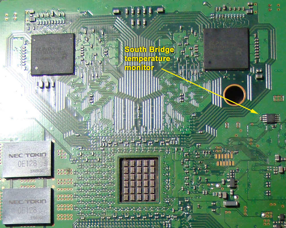
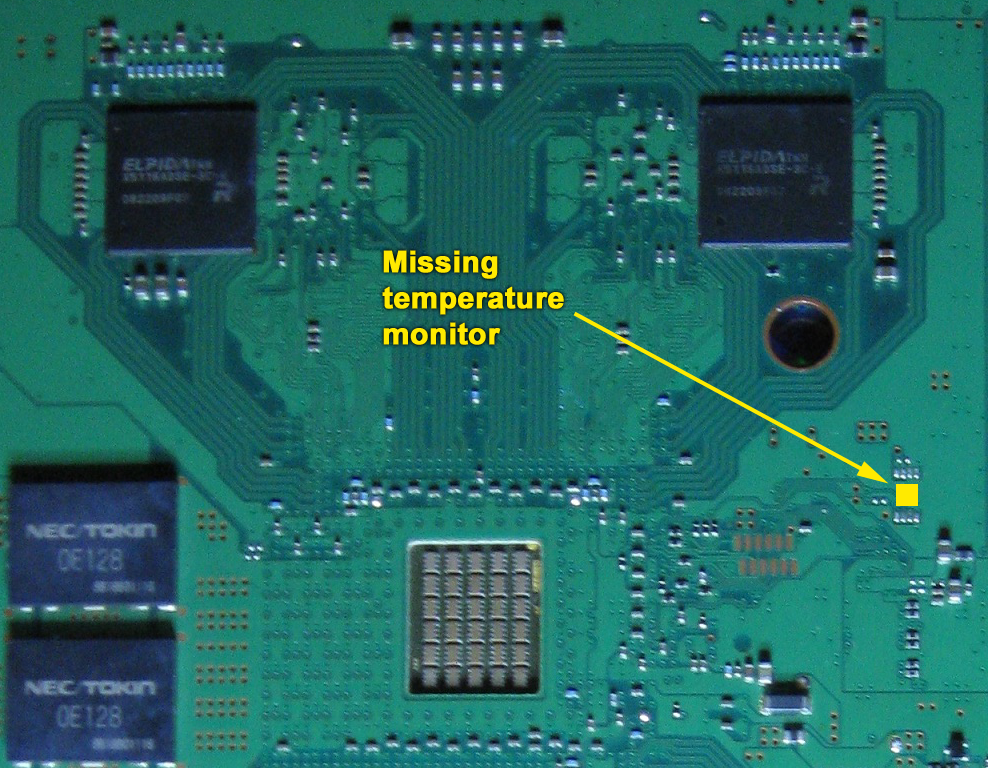
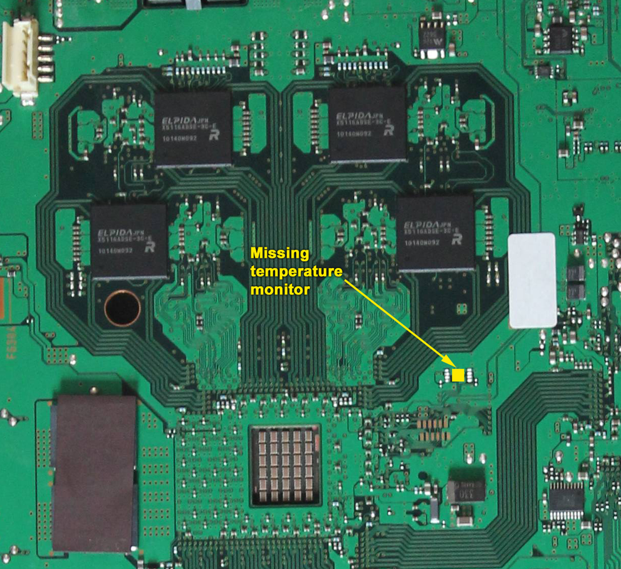
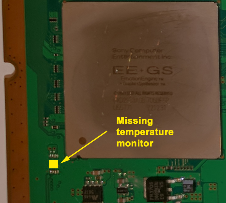
The circuit of the COK-001 and COK-002 is designed to install 5 temperature monitors... there are solder pads for them but only 3 are present (CELL/RSX/SB), im not going to post photos of them because most of you knows where are located and how they looks
The other 2 temperature monitors are located here:
We know his names because syscon shows them when we run the command "tzone", as example (this is different in other motherboards, only the COK's have 5)
Code:> tzone 00: 1st BE Primary 01: RSX Primary 03: BE VR 14: SB 15: EE+GS
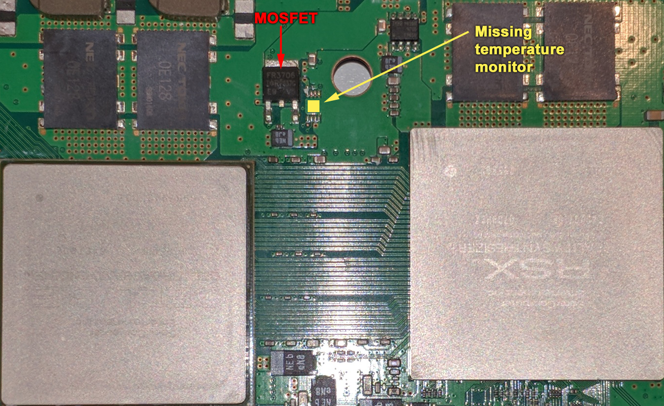
So... "BE VR" is the temperature monitor in between CELL and RSX (named IC6108 in the service manual), and is meassuring the temperature of:
1) The mosfet SUD40N02-08-E3 (named Q6310 in the service manual)
2) The voltage regulator BD3520FVM-TR at the other side of the motherboard (named IC6303 in the service manual)
Both components are the responsibles to generate the +1.2V_YC_RC_VDDIO line... but in your schematic you are drawing a single "dotted green arrow" to RSX (while the codename of this temperature monitor is "BE VR"... you know "CELL BE Voltage Regulator"
So my question is... are you sure they are feeding RSX only ?
The line +1.2V_YC_RC_VDDIO doesnt have any relationship with CELL ?
Or is just sony recycled the codename of "BE VR" to use it for "RSX VR" ?
As far i know there is not any mention of a temperature monitor named "RSX VR" in any syscon firmware, not even in pre-retail or the reference tool PS3 models, for curiosity sake, at bottom of this code we have a list of the output of the "tzone" commands in all documented PS3 models, as you can see the reference tool PS3 models have some temperature monitors that doesnt exists in retails, as example the temperature monitor named "XDR Primary" or "Air Intake" but not a single mention ever to "RSX VR"
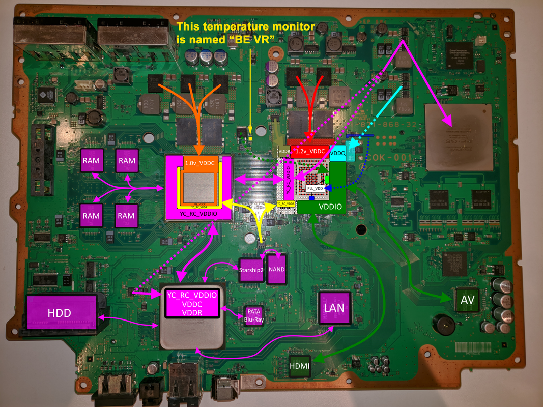
Nice, please advise me when you have something related with that components next to the "BE VR", i been wondering what means the codename "BE VR" since many time ago, the other day i was lurking the service manuals, photos, and your schematics of power lines and i hitted with this contradictionRight, that's a mistake and that picture needs updated. I will work up a new one. One that matches the same color scheme I have been using for the RSX pinout/voltage pics.
") ...or you could place it inside the PSU
...or you could place it inside the PSUhey that arrangement of resistors looks familiar."
"those values match up perfectly."
"So this is what they were doing. COOL!"
"Wow, they basically copied the exact same arrangement in the example, then sold millions of consoles...lol! I guess if the Manufacturer say's to do it that way, SONY does just that! At least you know it'll work. I mean, why reinvent the wheel and create potential issues when you have a working example right in front of you in the datasheet? Not a bad Idea really."
