You are using an out of date browser. It may not display this or other websites correctly.
You should upgrade or use an alternative browser.
You should upgrade or use an alternative browser.
vyktormvmpay25
Senior Member
Now done. I have recorded a bit in the link attached. Today is late for me going to sleep. I will reply more tomorrow.
http://s.go.ro/x52xeflx

Also on cell with black border is 1.03v power line.
http://s.go.ro/x52xeflx
Also on cell with black border is 1.03v power line.
RIP-Felix
Senior Member
1.75v may be the VDDQ and 0.9v the reference voltage, which according to this is VDDQ/2. The memory datasheets mentioned something about various reference voltages requiring a lower voltage from a divider. The Hynix date sheets says Vref = 0.7xVDDQ and that the nominal VDDQ is 1.8v. 0.7 x 1.8v = 1.26v. That's oddly close to the 1.2v the COK-001 schematic quotes for VDDR. I may be talking out my butt, or is any of this making sense?
Are there any markings on that IC? From the angle the pic is taken it looks like the chip was scrubbed, but sometimes that's just the angle of the camera. It would be nice if we could pull up the datasheet for that part, just to confirm it is the VRM. Too bad we don't have schematics to go off.
Are there any markings on that IC? From the angle the pic is taken it looks like the chip was scrubbed, but sometimes that's just the angle of the camera. It would be nice if we could pull up the datasheet for that part, just to confirm it is the VRM. Too bad we don't have schematics to go off.
RIP-Felix
Senior Member
HW side is still in the speculation phase ATM. Were just trying to explain differences seen in the 2 boards that had it does successfully. The software side still needs a user friendly firmware update to enable the Cell, without needing to remarry. I'm afraid that side of things is out of my skill set. I prefer to look at schematics, watch videos, and vomit speculative HW non-sense until something tangible comes from it.
We're all excited to figure this out though.
We're all excited to figure this out though.
Joonie
Developer
Thanks, your PS3 still has the original RSX: "rsx: b08 500/650 vpe:ff shd:3f [AP0005626:1:1:10:e:a:2:f:2][16:3:1:1:1:3:1][0:0:0]".
I just dumped mine, and looks like I have a very old one. (CECH-E01)
Code:
rsx: b02 500/650 vpe:ff shd:3f [4K0425501:1:3:17:2:9:4:f:2][39:2:1:1:1:3:1][0:0:0]Joonie
Developer
HW side is still in the speculation phase ATM. Were just trying to explain differences seen in the 2 boards that had it does successfully. The software side still needs a user friendly firmware update to enable the Cell, without needing to remarry. I'm afraid that side of things is out of my skill set. I prefer to look at schematics, watch videos, and vomit speculative HW non-sense until something tangible comes from it.
We're all excited to figure this out though.
I just spoke to a guy I know from Korea, and he also saw one of these guys from his customer as well. I wish he kept that lol
vyktormvmpay25
Senior Member
027810k

RIP-Felix
Senior Member
Yeah, I definitely was talking out my furry butt [BAD FELIX!}. I got Q6200 mixed up with IC6200. Different things altogether. That is related, some kind of DDR Termination...reference...voltage thingy...IDK what, I'll have to stare at it some more as it looks to be related to whatever the added resistors are doing.
I made this to visualize the changes we're talking about:

It's hard to tell if R6219 was removed or still in place. @LeoTW630 The photo is too small. It would be nice if we could get measurements, the resistance (ohms) of R6214 and R6216 that were added, and a higher resolution image of IC6200 to confirm the part was changed to the BD3504FVM-FTR. This way we be sure how to replicate the mod. It's just hard to be sure with those pictures.

@DeadEnd I'm starting to arrive back at the work you did looking at the schematics of those 2 VRM and calculating the Resistor values. It's getting late and I'll have to pick it up tomorrow, but maybe you can reiterate what values you thought and why.
I'm also curious if the BD3504FVM-FTR is used on a 40nm console and that's why they did this. So @vyktormvmpay25 could you find that IC and image it? Should be on reverse side of the board next to the Tokins (basically the same place your were looking but on the reverse side of the board). Sorry I had you cut that heatsink. At least now you can get at the bypass caps easier...lol. I still need to get the voltage of the VDDR (pin 6). That way we can compare it to a COK-001 stock to see if this VRM swap is necessary, or because the D3502 was bad and they only had D3504's on hand. I'm guessing they did it for a reason.
I made this to visualize the changes we're talking about:
It's hard to tell if R6219 was removed or still in place. @LeoTW630 The photo is too small. It would be nice if we could get measurements, the resistance (ohms) of R6214 and R6216 that were added, and a higher resolution image of IC6200 to confirm the part was changed to the BD3504FVM-FTR. This way we be sure how to replicate the mod. It's just hard to be sure with those pictures.
@DeadEnd I'm starting to arrive back at the work you did looking at the schematics of those 2 VRM and calculating the Resistor values. It's getting late and I'll have to pick it up tomorrow, but maybe you can reiterate what values you thought and why.
I'm also curious if the BD3504FVM-FTR is used on a 40nm console and that's why they did this. So @vyktormvmpay25 could you find that IC and image it? Should be on reverse side of the board next to the Tokins (basically the same place your were looking but on the reverse side of the board). Sorry I had you cut that heatsink. At least now you can get at the bypass caps easier...lol. I still need to get the voltage of the VDDR (pin 6). That way we can compare it to a COK-001 stock to see if this VRM swap is necessary, or because the D3502 was bad and they only had D3504's on hand. I'm guessing they did it for a reason.
vyktormvmpay25
Senior Member
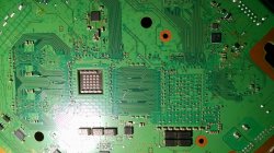
First is point of 1.75v. Mark area. I can not see any mosfet driver. Last photo is around av ic and hdmi ic on bottom but it is connected on that area.


From a scrap board grey is 1.8v(1.75)

I may compare pins with scrap board from now I have to assembly for testing. I still have 2 3000 for reball this week.
From a scrap board grey is 1.8v(1.75)
I may compare pins with scrap board from now I have to assembly for testing. I still have 2 3000 for reball this week.
Last edited:
DeadEnd
Senior Member
Awesome progress guys.
Btw, here is another helpful guide for testing voltages on COK-002. (I am not fully focused on what is going on in this thread at the moment as I've got a lot of school stuff going on. So I'm just throwing this out there for now. )
https://www.trisaster.de/page/index.php?topic=459
As to syscon firmware updating/dumping. At least the EEPROM dumping part is somewhat clear (well, as clear as it can be until the user "maj4r" clarifies the steps which I have outlined ).
@DeadEnd[/USER]
It's hard to tell if R6219 was removed or still in place.
I'm starting to arrive back at the work you did looking at the schematics of those 2 VRM and calculating the Resistor values. It's getting late and I'll have to pick it up tomorrow, but maybe you can reiterate what values you thought and why.
I'm also curious if the BD3504FVM-FTR is used on a 40nm console and that's why they did this.
I think R6219 is there, but with a new value. But notice that if BD3504 is used, on top of replacing R6214 and R6216 you'd also have to replace 0 ohm resistors R6219 and R6222. And here is something I have overlooked entirely. Since I am dealing with european models, I have just noticed that, for instance, IC6602 (which uses BD3504) is configured slightly differently on COK-001. I must be careful to not mix up these two schematics from now on... And the difference is, again, in the resistors around Vfb and Vd. In COK-002 they deviate from the standard 3300 ohm and there is extra 470 ohm added in series, making R2 in that circuit around 3770 ohm and give Vfb pin 0.610v. But in COK-001, there is only 180 ohm added in series, which turns resistance of R2 into 3480 ohm and gives Vfb 0.634v. However if you look at the datasheet again, 0.634v is still within tolerance:

Now another thing you could take into the equation is that IC 6602 is driving a different mosfet compared to IC6200. Also Vd pin follows the same resistor logic as Vfb. Perhaps, you can look into that and maybe that is what causes different values of R2. However, it seems strange as both COK001 and 002 use the same mosfet at IC6602, yet the values still change (from 180 to 470)...
In any case, let's say you are trying to accomplish 1.2v with BD3504, you could probably just go the recommended route and install R6219 and R6222 as 3300ohm (or 3480 ohm if you happen to find that value in one resistor), while R6214 and R6216 will have to be 3900 ohms.
Here is how you would do it in practice (and possibly what Sony technicians did to that board):

But even if we find out that there has been no changes to 1.2v, perhaps that original IC 3520 was deemed unstable over time or unstable for hynix memory on 40nm rsx, and a more reliable BD3504 (or whatever was used in slim model) was put in its place?. So it would be up to the user to decide if they wanna mess with it or not. Of course best way to know for certain would be by measuring the resistors on the modified board...
"Sigh", I wish I had gone for electrical engineering studies instead of mechanical...
Now another thing you could take into the equation is that IC 6602 is driving a different mosfet compared to IC6200. Also Vd pin follows the same resistor logic as Vfb. Perhaps, you can look into that and maybe that is what causes different values of R2. However, it seems strange as both COK001 and 002 use the same mosfet at IC6602, yet the values still change (from 180 to 470)...
In any case, let's say you are trying to accomplish 1.2v with BD3504, you could probably just go the recommended route and install R6219 and R6222 as 3300ohm (or 3480 ohm if you happen to find that value in one resistor), while R6214 and R6216 will have to be 3900 ohms.
Here is how you would do it in practice (and possibly what Sony technicians did to that board):
But even if we find out that there has been no changes to 1.2v, perhaps that original IC 3520 was deemed unstable over time or unstable for hynix memory on 40nm rsx, and a more reliable BD3504 (or whatever was used in slim model) was put in its place?. So it would be up to the user to decide if they wanna mess with it or not. Of course best way to know for certain would be by measuring the resistors on the modified board...
"Sigh", I wish I had gone for electrical engineering studies instead of mechanical...
Btw, here is another helpful guide for testing voltages on COK-002. (I am not fully focused on what is going on in this thread at the moment as I've got a lot of school stuff going on. So I'm just throwing this out there for now. )
https://www.trisaster.de/page/index.php?topic=459
As to syscon firmware updating/dumping. At least the EEPROM dumping part is somewhat clear (well, as clear as it can be until the user "maj4r" clarifies the steps which I have outlined ).
Last edited:
RIP-Felix
Senior Member
Yeah, I must have been tired, that's the N-MOSFET it's driving.I got Q6200 mixed up with IC6200. Different things altogether. That is related, some kind of DDR Termination...reference...voltage thingy...IDK what, I'll have to stare at it some more as it looks to be related to whatever the added resistors are doing.
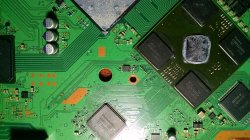
Looks like the BD35282. Closest thing I could find in a quick search is BD35281. They might have gone this approach to minimize components. Seems similar in construction to the others except it has the MOSFET inside. Where is this on the board? If it's close to the RSX that could be what we're looking for.From a scrap board grey is 1.8v(1.75)
I think that 1.75v you measured is the VDDR. I was originally thinking we needed to confirm that voltage on a 65nm and 90nm board, but not I'm pretty sure these linear regulators are all either set (with resistors) or fixed to 1.2v anyway. How that ends up coming out to ~1.8v is still witchcraft to me, but whatever.
I think that second console had some problem with the D3520 on the original COK-001 (perhaps too much noise), so they changed it to the D3504 seen in the pics, which required them to set the voltages with the resistors added. This seems to just be another way to accomplish the same goal, so I'm not sure it's necessary to switch the components out unless there's some kind of problem. All the datasheets for the onboard memory have the same voltages and noise. So long as a COK-001 has 1.8v +/- 25mV on the VDDR line, it should be okay for the swap.
We should still probe VDDR with an oscilloscope for nominal voltage and noise (Vpp) on 40nm, 65nm and 90nm consoles. Just to dot our i's and cross our t's. I expect them to be the same ~1.8v (+/-)25mV. Then I'd say we're ready for an attempt.
RIP-Felix
Senior Member
@vyktormvmpay25 Try here:

That's not too far away from the RSX. On the COK-001 there was a large contact landing pad labeled + on the schematic. I'm guessing that's for QA in the factory. There is one there in your pic too. I'm betting that's the equivalent on your board. Probe it and see if you get the 1.2V I've been expecting. If you have an oscilloscope, could you measure the noise too?
That's not too far away from the RSX. On the COK-001 there was a large contact landing pad labeled + on the schematic. I'm guessing that's for QA in the factory. There is one there in your pic too. I'm betting that's the equivalent on your board. Probe it and see if you get the 1.2V I've been expecting. If you have an oscilloscope, could you measure the noise too?
Last edited:
vyktormvmpay25
Senior Member
My osciloscop is on another workshop atm. May take time, already assembled this motherboard. I will test when I reball another motherboard if is not reported by then. I can do voltage check tomorrow when I have this unit with all games ready. I will take bottom plate off and assemble in test mode.

ElGris
Senior Member
Could you show me from where should I get those readings?We need to test 1.2v at the *VDDR line which goes to memory on RSX. Unless you know which points to test, I suppose you could start with taking hi-res pictures of the board, especially areas around RSX. Both sides.
Attachments
vyktormvmpay25
Senior Member
Just a second. Can you work with board open? I going to find 1.2v on my board.
Edit :
@RIP-Felix there is 1.5 v on there.

Going with syscon test later just curious about. Left mobo in test mode.
Done last photo with all voltages.
@ElGris superslim must be assembled as mine or something similar in order to power and take measurements. I is quite risky to do it. I will think on something to start in test mode.


Edit :
@RIP-Felix there is 1.5 v on there.
Going with syscon test later just curious about. Left mobo in test mode.
Done last photo with all voltages.
@ElGris superslim must be assembled as mine or something similar in order to power and take measurements. I is quite risky to do it. I will think on something to start in test mode.
Last edited:
RIP-Felix
Senior Member
Could you show me from where should I get those readings?
That looks like a juicy target. But if there is a schematic for your motherboard revision, look up the RSX and be sure that's it.
DeadEnd
Senior Member
That looks like a juicy target. But if there is a schematic for your motherboard revision, look up the RSX and be sure that's it.
There are no schematics past SEM-001 boards.
The actual MFW needs to contain a syscon patch which patches the EEPROM handling functions, just as an example:
The patch structure is documented here: https://www.psdevwiki.com/ps3/System_Controller_Firmware#PTCH_Firmware_TOC, you can also find a decoding script here: https://pastebin.com/xGDH6taM .Code:COK-001 0x1FDA2: 3D E0 8B 49 0x41334: 00 00 00 00 0x41338: FF 7F 00 00 DIA-001 0x20512: 3D E0 8B 49 0x4B814: 00 00 00 00 0x4B818: FF 4F 00 00 DIA-002 0x206A2: 3D E0 8B 49 0x4C284: 00 00 00 00 0x4C288: FF 4F 00 00
The encrypted patch structure can be found here: https://www.psdevwiki.com/ps3/System_Controller_Firmware#Header.
So I got the syscon pkg files out of PUP. Trying to use your examples for COK-001 (According to psdevwiki it's in the file SYS_CON_FIRMWARE_01000006.pkg) I ran it through hex editor and I for the life of me cannot find those offsets. I even decrypted it using your script, still I don't see them. You gotta give us more explanations man.
Last edited:
vyktormvmpay25
Senior Member
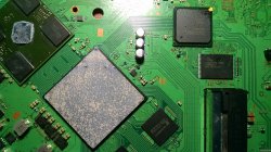
Rip-Felix meaning that ic D35287 schematic.
M4j0r
Developer
So I got the syscon pkg files out of PUP. Trying to use your examples for COK-001 (According to psdevwiki it's in the file SYS_CON_FIRMWARE_01000006.pkg) I ran it through hex editor and I for the life of me cannot find those offsets. I even decrypted it using your script, still I don't see them. You gotta give us more explanations man.
I didn't provide a script for the patch decryption, only one which parses the decrypted patch to visualize the content (it decodes the decrypted version).
First you have to decrypt the pkg and then the content of the pkg, then you have the patch. unpkg is used for the pkg and zecoxao released the patch decryption tool.
And the offsets are of course not part of the patch, these are for the firmware, but are also instructions for the patch - where does the data need to be written to and what data?
You even quoted that link: https://www.psdevwiki.com/ps3/System_Controller_Firmware#PTCH_Firmware_TOC. It has four "PTCH Addresses" and four "PTCH #x Instruction / Data". Address is where the address goes and Instruction/Data is where the data goes - just be aware of the endianness.
You can then check your patch using https://pastebin.com/xGDH6taM .
I advise you to not install a new modified PS3 system firmware without having a way to recover from it, same goes for a syscon patch.
The offsets/data that I provided for the syscon patch are safe. If you just want to enable the full eeprom access over UART, you don't need the first patch, that's just for the CELL side.
Similar threads
-
-
 PS3 PS3 CECHA RSX Swap (40nm) – JP Limited – SYSCON Patch, VDDC Mod – Need Detailed Help
- Started by jw0710
- Replies: 4
-

-
