DeadEnd
Senior Member
Here's the overview of voltages on RSX that you may see when probing different points.
1 +1.8V RSX_PLL_VDD (voltage for clock multiplier?)
2 +1.2V RSX_VDDC (main supply voltage)
3 +1.2V RSX_VDDR (memory voltage)
4 +1.2V YC_RC_VDDIO
5 +1.5V RSX_RC_VDDA
6 +1.5V RSX_VDDIO
7 +1.8V RSX_FBVDDQ (memory buffer voltage)
Based on this: https://www.psdevwiki.com/ps3/Talk:RSX
From my understanding, all these lines go into RSX and are, in theory, supposed to be present on all models. The point was still to try and figure out if VDDR actually differs between revisions. I bet that 1.5v @ElGris and @vyktormvmpay25 were seeing is not VDDR, but VDDIO or VDDA. Felix could correct me here since I have a tendency to overlook important logic...
I also just discovered a very raw voltage scheme for DYN-001 (it's still using 65nm RSX), but it claims there may be errors and main supply to GPU is missing. So the schematic is only good for checking IC names.
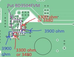
@ElGris, I have posted here some thoughts about resistors earlier on. If you're talking about the ones related to reset, it was mentioned here
At this point I think many have noticed I'm nearly thinking aloud. Like Felix said, it would be much easier if we had a EE checking voltages and helping with schematics.
1 +1.8V RSX_PLL_VDD (voltage for clock multiplier?)
2 +1.2V RSX_VDDC (main supply voltage)
3 +1.2V RSX_VDDR (memory voltage)
4 +1.2V YC_RC_VDDIO
5 +1.5V RSX_RC_VDDA
6 +1.5V RSX_VDDIO
7 +1.8V RSX_FBVDDQ (memory buffer voltage)
Based on this: https://www.psdevwiki.com/ps3/Talk:RSX
From my understanding, all these lines go into RSX and are, in theory, supposed to be present on all models. The point was still to try and figure out if VDDR actually differs between revisions. I bet that 1.5v @ElGris and @vyktormvmpay25 were seeing is not VDDR, but VDDIO or VDDA. Felix could correct me here since I have a tendency to overlook important logic...
I also just discovered a very raw voltage scheme for DYN-001 (it's still using 65nm RSX), but it claims there may be errors and main supply to GPU is missing. So the schematic is only good for checking IC names.
@ElGris, I have posted here some thoughts about resistors earlier on. If you're talking about the ones related to reset, it was mentioned here
Observation 1: R2153 is removed and bottom pin of R2054 is 'shifted' to nearby ground:
As for the IC and the surroundings resistors, for now the most likely conclusion is to leave it untouched. But what POSSIBLY happened might have been this:
At this point I think many have noticed I'm nearly thinking aloud. Like Felix said, it would be much easier if we had a EE checking voltages and helping with schematics.
Last edited:


