Ok, i see what you mean, btw another way to identify which one is each is to look at the "SW_xx" signals, thats syscon outputs to enable the chips, and that names are respected in all the manuals we have (and probably some of them exists with the same names even in PS3 superslim models)
What i meant is the component in this image is also a SN105233DBTR (labeled as IC6301)
But i didnt realized in SEM-001 there are two SN105233DBTR
I just realized, this service manuals are a pain to navigate, btw, someone thought in editing them to improve that shitty bookmarks/index ?, everytime i need to search something i have to scroll all the pages just trying luck
Awesome, so that pads named PF1 and PF2 in the COK-001/2 manuals seems to be something that was ready to be used since day one but was not used in COK-001/2, i wonder if there is some mention about them in the BCU-100 manual or if is inherited from pre-retail prototypes... never minds, right now i dont have the courage to dig so deep
Yeah, let me reword it, im not a native english speaker but im going to try to simplify it, also for all you to tell me if is right and/or improve it
In COK-001/2 the component named IC6302 is switched by syscon signal SW_2 and is intended to generate +1.8V_VDD_MEM only
In SEM-001 the component named IC6302 have a pin switched by syscon signal SW_2 intended to generate +1.8V_VDD_MEM ... and also have another pin switched by SW_8_A that seems to be intended to generate +1.2V_BE_VCS
So the hack involves picking in the SW_8_A (but dont cut it because is responsible for other voltages) and use a SN105233DBTR to copy what the SEM-001 is doing to generate the +1.2V_BE_VCS
I know... there are more signals involved, is not so easy but i guess most of this components can be recycled from scrap boards, the SN105233DBTR exists in COK-001/2 (one unit) and SEM-001 (2 units)... probably the DIA-00x motherboards have a couple too because was using a 65nm CELL
Yes, that actually seem doable. We just need to add the voltage regulator and bypassing to the interposer. Then a few breakout pads for routing signals and perhaps a few choice ones for diagnostics.
Once we have a 65nm pinout, we can overlay and compare to the 90nm layout. That will tell us which pads need to be re-routed. Then an interposer could be designed. After that, it's up to the software gurus to figure out the SYSCON changes and training.
OMG I have an knowledge gasm with that, I mean we all Crazy Crazy see Cell Broadband Engine 45nm on Fat PS3, including Felix, Thank you so much Sandungas on your WorK on that.
Yes, that actually seem doable. We just need to add the voltage regulator and bypassing to the interposer. Then a few breakout pads for routing signals and perhaps a few choice ones for diagnostics.
Once we have a 65nm pinout, we can overlay and compare to the 90nm layout. That will tell us which pads need to be re-routed. Then an interposer could be designed. After that, it's up to the software gurus to figure out the SYSCON changes and training
Hey Félix how are you? Im the """batman" that told computer Booter tô pay respect tô you, anyways I also asked here tô know if we could Try install 45nm Cell on Fat PS3 so I Would say lets told everybody that uses the Cell Swap with newer ones that these Mods Are Not To Be made On Any Working Machines!!! Only on Deffective Ones to do the Mod as an Repair Thing, I think we pretty Agree on That Félix and Maybe Sandungas agree too!! I mean we Love Cell Broadband and PS3 and watching Computer Booter Moding Working 100% Ps3s and the killing them is a big PAIN and loss no matter if slim or fat.
Please can someone Please make the Frame Rate Measurer WorK on Ps2 neto emu and Please Unlocked frank Rate on Ps2 Emu, This Will Finaly show Cell Broadband Full Power As an Computacional Cpu on Stardart Cpu tasks, I mean Acording tô devwiki 7 Entire Spes and the 1 Ppe and 2 Threads of It are All Dedicated tô PS2 Emulator, and well and Q6600 at 3.3.2ghz with 4 Cores can bê used 100% by Pcsx2 by only Running Gran Turismo 4 original at 60 fps só if we had PS3 -ps2 Emu with Unlocked Fps We could finally see all performance from Cell B.E, Please Someone lets Try this please, im highly expecting Cell to Achieve 130Fps on Gt4 Emutated on Ps2 net Emu.
Well I've been trying to write out the connections out of both Cok and Sem manuals into Excel. Let me know if you are also working on that because I already started a little bit.
Well I've been trying to write out the connections out of both Cok and Sem manuals into Excel. Let me know if you are also working on that because I already started a little bit.
No, you can continue doing that list of displaced pads because your work doesnt "overlaps" with what im doing, are actually complementary, and eventually we can add all that pinout info in wiki to make room for descriptions of every pin, etc...
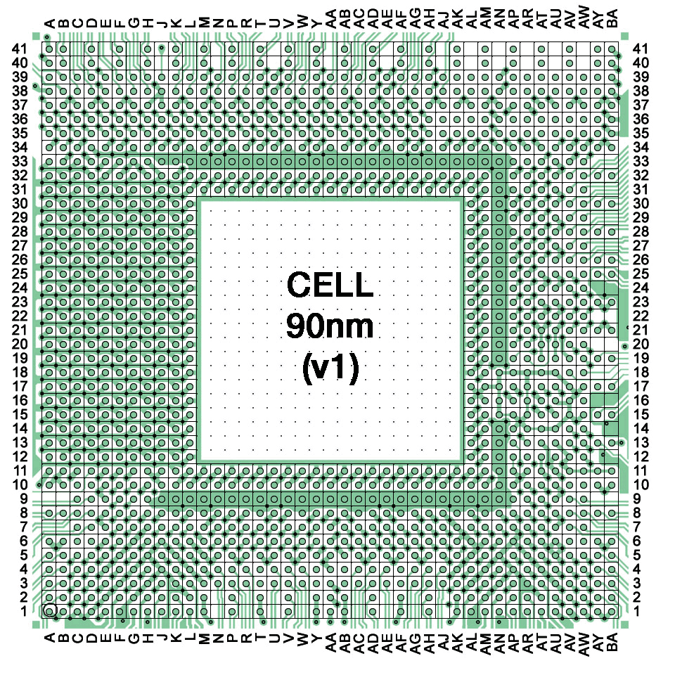
My interest in all this is a bit long to explain, i would like to rebuild some wiki pages related with CELL and i need to make high quality images of the pad layouts
As you can deduce i already invested some time in it (since many weeks ago), but right now im at a point where i realized i need to rebuild them entirelly from scratch at 3x his size because the actual images (used in the gif) are made using a grid with a cell size of 20x20px (is not posible to write text inside the cells)
In other words.. the gif i posted was made at 960x960px and i need to repeat it at 2880x2880... this results in "cells" of 60x60 pixels (to write 2 rows of text inside each cells with a 8px font)
Also, i decided to "draw" the circuit entirelly from scratch for all them
Anyway, i already made some more progress than what im showing, but this "project" to do high quality images is freezed by now... but after spending some time looking at it i can guide you in your list, im going to mention some details (that you should confirm) to check, all this is applyed to the designs of the CELL 90nm and 65nm only
Btw, if i had to bet... i would say the CELL 45nm is almost exact than the CELL 65nm... the only difference seems to be in the "inner ring" but thats power and gnd pads
-At north of my images is located the data bus for RSX (the infamous FlexIO), all the lines matches in between 90nm and 65nm, it takes most of the pads from rows 38,39,40,41 (board side A) and rows 35, 36 (VIAS to board side B)
-In 90nm the right side of the FLexIO bus have a lot of pads unused/reserved... as far i understand it seems they was intended to create a higher bandwith bus with a more powerful RSX (IBM stuff, not used in retail PS3 models). In 65nm this pads has been repurposed for the SouthBridge bus
-At most left border of the FlexIO there are 3 or 4 control pins that doesnt matches
-There is also one of the "power rails" at left from the tokins (the most closer to the FlexIO) that doesnt matches
-At south of my image is the RAM data bus (rows 1,2,3,4,5,6,7,8,9,10)... you know... are really 16 groups of 8 pads each that spreads outside of CELL "grabbing" the RAM chips as an spider... his pad locations can be seen very well differenced in groups of 8+8 (half of them goes to VIAS to the other motherboard side)... this area at bottom is pretty much simmetrical left<--->right. And it seems to match fine in between 90nm and 65nm (it seems they refused to change anything in this area related with the RAM pads). The only posible difference worthy to be mentioned is at the bottom-center pads (row AA/1,2,3,4,5,6)... some of that pads are control signals
-The problem is at right side of my images... to simplify the story... in 90nm the SB data bus was located in a squared area touching the right border rows 26,27,28,29,30,31,32 and on top of it (rows 34,35,36,37,38,39,40,41) there was a lot of pads "unused" from the FlexIO
In 65nm they moved the SB "up", to rows 34,35,36,37,38,39,40,41
I think this is the real reason why they changed the CELL pad layout from 90nm to 65nm... they realized the "reserved" pads at the most right of the FlexIO interface was pointless
-And the next problem (this is going to be much more tricky to identify) is in the 90nm most of the pads at the right side are control signals (usually in groups of 2, 3 or 4)... but as a result of the room recovered by moving the southridge bus "up" probably a lot of them was reorganized
-In 90nm the right side of the FLexIO bus have a lot of pads unused/reserved... as far I understand it seems they was intended to create a higher bandwith bus with a more powerful RSX (IBM stuff, not used in retail PS3 models). In 65nm this pads has been repurposed for the SouthBridge bus
...
I think this is the real reason why they changed the CELL pad layout from 90nm to 65nm... they realized the "reserved" pads at the most right of the FlexIO interface was pointless
I'm making my way through some of the docs @DeadEnd found, and one of the things I'm seeing is that FlexIO got it's name because it's supposed to be "flexible", meaning, it can be reused for to talk to various other devices (even another Cell), without needing to design even more interfaces. It was reporpused, yes, but that's kinda the point of the FlexIO interface. So I don't know that it was "pointless" as much as just choosing which interfaces to connect to.
As a slight tangent, that was the point for the bit-training too -- Cell itself runs under 3 different clocks, and the external interfaces could be running at one of those different clocks, so bit-training needs to happen so all the clocks are in sync.
Let me put this into numbers, i mean it was pointless to have 54 pads of the CELL 90nm "unused" (not connected to anything) in the PS3 retail production, but im not telling it in an offensive way like if they suddenly realized about it
They was very aware of it, but is a decission made by IBM because the original CELL 90nm was designed for other devices
In total, the CELL 90nm is designed with 180 pads dedicated to the FlexIO (RSX) divided in 10 groups of 18 pads each (where half of them goes into VIAS to "board side B"), but the COK-001/2 implementation only uses 7 groups of 18 pads each
In other words.. the COK-001/2 circuit is designed to use only 70% of the FlexIO pads from the 90nm CELL
In total, the CELL 90nm is designed with 180 pads dedicated to the FlexIO (RSX) divided in 10 groups of 18 pads each (where half of them goes into VIAS to "board side B"), but the COK-001/2 implementation only uses 7 groups of 18 pads each
Im not sure if is technically correct to use the term "channel", but im going to use it to comment some interesting details, lets say every group of 18 pads is a channel
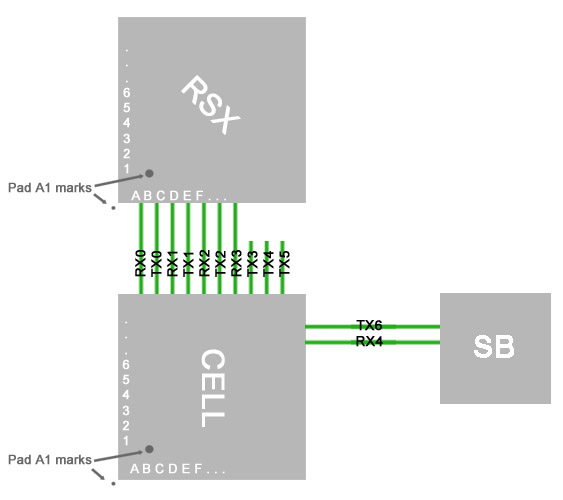
As mentioned before, it seems the FlexIO of the 90nm CELL is composed by 10 channels in a straight line, if we start from top-left corner in my gif and count the channels in clockwise direction are codenamed:
RX0 (18 pads to RSX)
TX0 (18 pads to RSX)
RX1 (18 pads to RSX)
TX1 (18 pads to RSX)
RX2 (18 pads to RSX)
TX2 (18 pads to RSX)
RX3 (18 pads to RSX)
TX3 (unused)
TX4 (unused)
TX5 (unused)
But... if we turn the corner in clockwise direction (at the right border) we have
TX6 (18 pads to South Bridge)
RX4 (18 pads to South Bridge)
Hmmm... the protocol seems to be the same in RSX and SB, using groups of 18 pads for Tx and Rx so im wondering if we should consider the South Bridge is located "inside" the FlexIO ?
In that case the FlexIO in the CELL 90nm have 12 channels ?
------------
Anyway... the change they did in between CELL 90nm to 65nm when they moved the Southbridge pads "up" matches a bit with the location of the "unused" channels and is making me wonder if they make it match with the exact position of a couple of those "unused" chhannels in the CELL 90nm
Right now i cant tell because i have not dedicated much time checking the related pads but thats a huge problem for the frankenstein experiments
Edit:
Btw, the channel names can be seen in this image made by kiaw
Are added "outside" of the grid (written verticall from top to bottom at most left border), but his location is just orientative, keep attention at how he interleaved the colors of that pads, every color indicates a channel (18 pads)
7 channels in total: RX0, TX0, RX1, TX1, RX2, TX2, RX3
4 channels in direction CELL--->RSX
3 channels in direction CELL<---RSX
Can't follow what you're on about at this point. But I have nearly finished Excel spreadsheet of every contact for 90nm Cell. It's going to be more difficult to do the same for 65nm though ,because the pins are grouped differently.
Can't follow what you're on about at this point. But I have nearly finished Excel spreadsheet of every contact for 90nm Cell. It's going to be more difficult to do the same for 65nm though ,because the pins are grouped differently.
The pad/functions have 2 different names... one of them is the name of the CELL pad, and the other is the name of the signal connected to the CELL pad... most of the times the names matches, but in this specific case (in the data buses of RSX/RAM/SB) the names doesnt matches
The names of the signals connected to the CELL pads are confusing... but if you look at the names of the CELL pads you are going to see is mentioned "TX0_TXN1" and "TX0_TXP1" (in pairs "N" and "P")...or... "TX0_TXN8" and "TX0_TXP8" ... or... "RX2_RXN0" and "RX2_RXP0" ... etc...
This names indicates very well how are grouped in "channels" (18 pads each) and how are paired
The pad/functions have 2 different names... one of them is the name of the CELL pad, and the other is the name of the signal connected to the CELL pad... most of the times the names matches, but in this specific case (in the data buses of RSX/RAM/SB) the names doesnt matches
Sorry, im looking at the manual and the names matches, so the identification of the channel names and the pairing of wires is straightforward, what i explained is valid but probably you already realized about it . Is going to be seen better in your excel by "sorting" the rows by his names
*The weird/confusing names are the pads for the RAM data bus, using names like "Y0" and "Y1" ...or... "DQ0" and "DQ1" (together with a number indicating how are grouped)
I dont know what means that DQ and Y references... i guess is because the RAM protocool is different than the FlexIO
I bet Y is going to refer to XDR Ram. A quick google search says that the previous name for xdr was yellowstone. I thought I'd seen that referenced somewhere in the docs, but I'm AFK right now and can't find it.
Here's one article I found, from around that era.There's more, too
I would like to report another issue that is unusual and is CPU related. Random shutdown because of a slight flex under Cell. As in, boots for a few seconds into XMB, all good, then "bang", straight shutdown. No YLOD, no warning. Just straight to standby. Tried with different PSUs. While lifting RSX, my heater seems to have caught the side of the Cell... Maybe there was moisture, either ways, there was a very slight warp on the board and balls looked more squished... But only very slightly. I remember there was some shutdowns when I was testing ripple, but at the time I attributed it to PSU not being screwed in. Later I kept testing more and didn't see any problem. I played on it for hours at a time. No issues at all... Then I closed it up and thought it was all good. So I turn it back on and suddenly shutdowns. I couldn't figure out what could cause it until I noticed my USB stick was not plugged in. I plugged it back in and no more shutdowns. The usb is one of those fake "gold" ones, which weighs idk how many gramms, but significantly heavier than a plastic one. I held its weight with a hand and shutdowns reappeared. Syscon only caught 1001 errors. So then I reflowed CPU and no more shutdowns without USB stick. However, I didn't actually "reflow" it all the way. I was too careful with temperatures thinking it would die. Anyway I eventually lifted it for a reball... It seems to have required 10C higher temperature profile than RSX. I only managed to lift it at 240 C. The smell was unbearable.
Which is what brings me to the point of why I'm losing interest in the mod. You can't win with these boards, maybe one time goes well but another time you accidentally damage something else. Sure, my top heater was a bit too wide... Not the best. Ironically the only board that has no problems since the swap has a 65nm GPU installed. I have big respect for Victor and others who have limitless patience for these type of things, but I'm not exactly a fan of reballing. I lift 90nm without worrying about killing them if they're already dead anyways, and 40nm usually isn't so sensitive. But lifting a Cell at such high temperatures with caps that are easily messed on the back and hoping it stays alive after it all is just one extra task I didn't plan on doing. This is starting to feel masochistic.
Haha... Yes, this is me after each reball! It's an ardous process. These consoles are fragile.
I feel like quitting after each fail, and elated after each win. This is one of those super hard challenges that exploit our emotions. One where we feel inadequate when it doesn't work, like it'll never become easier. But that's just because it's a difficult task. Theres nuances and new ways for things to fail. Each time Murphy pops up his fuggly head is yet another setback. It feels more significant. But really, it's just another lesson requiring a strategy to mitigate.
To protect the CPU and other components I mask it off and only expose the RSX. I think that helps to prevent warping. That and the jig.
But no matter how confident I get after win, I just know the next one is going to humble me. These boards are fragile and this process hard on them. We have to expect that some % just cannot be saved and it's not something we did or didn't do. Some are just suicidal.
@sandungas@RIP-Felix I have completed the Excel sheet for the 90nm CELL. It is entirely based on the service manual. Sadly my patience has run out for the 65nm, so maybe one of you could continue (In the SEM datasheet they did not group the pins alphabetically but by function, so have fun with that ).
I've tried to mark important notes as well as I could. For the voltage pins I put in parenthesis the name of the contact that it connects to on board (which does include voltage value in its designator). But yeah, feel free to use this to build a better image of Cell's layouts or whatever.
The file is in this folder among all the other documents with regards to Cell's designs https://bit.ly/3Ir1Cha


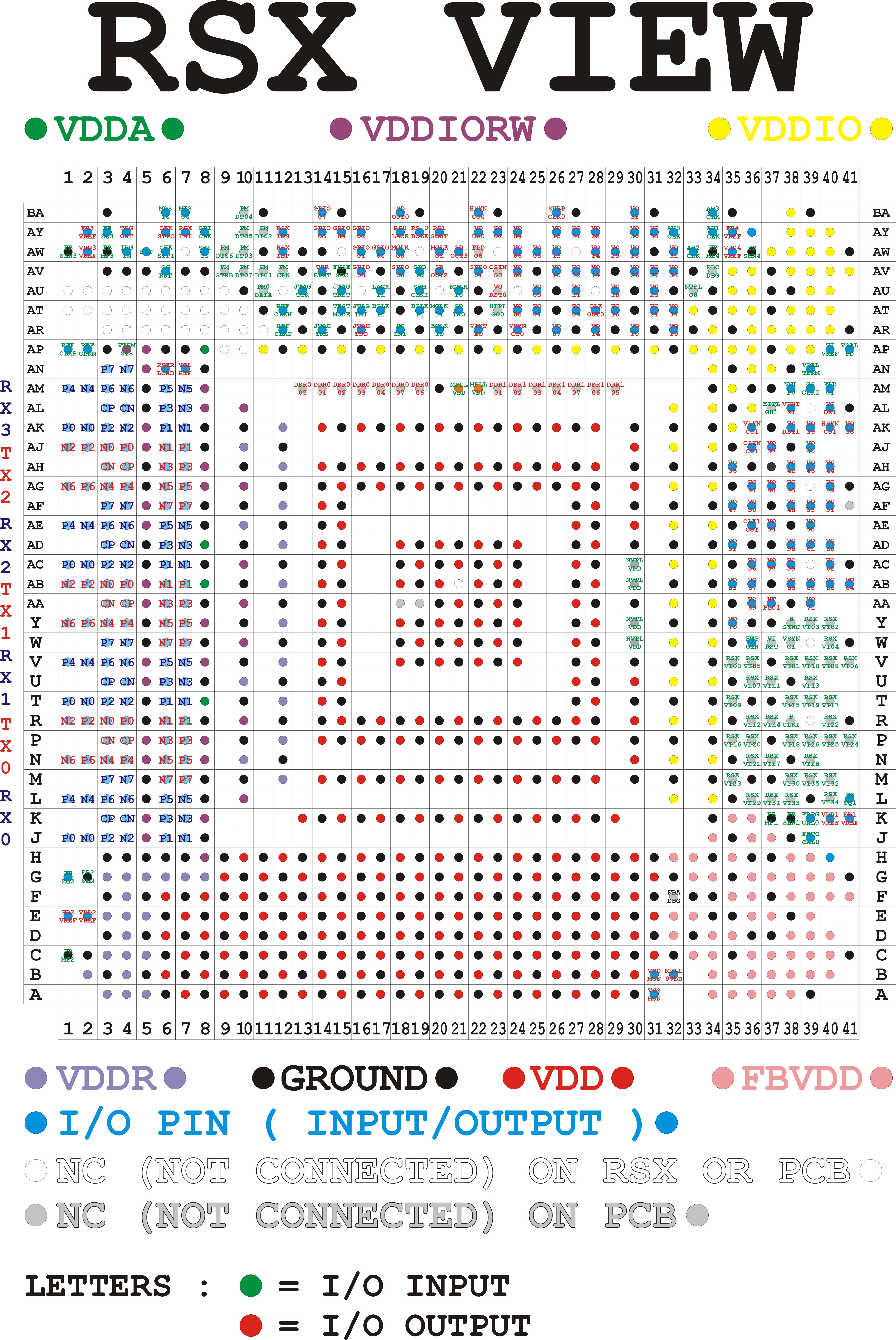
")