PS3 Motherboard Ver-001 with pad B0 ripped where can i make a jump?

Vitor Leão

Forum Noob
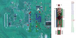
Hello a friend gave me a Ver-001 board with the pad B0 completely destroyed.
ixhtnli-jpg.19473

I couldn't find any schematics/diagrams of this model thus i'm in need of help.
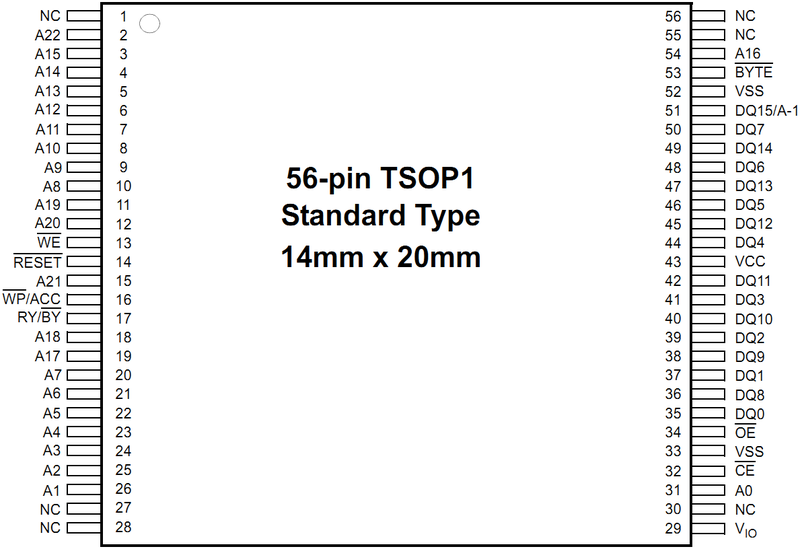
I need to know where to jump the nor chip pin A16 to. The only thing i know is that it seems to be going to the South Bridge chip true one of the under/middle layers of the board but don't know where/if it reappears somewhere else.
Even if there isn't a Pad where i can make a jump to i can try to make it under the South Bridge chip itself if i know with pin on the chip its going to but jumping to a pad would be much easier. The South Bridge chip is the CXD2984AGB.
The PS3 still turns on and seems to be "working" but gives no video and the RSX chip is not heating. After some research the pin A16 seems to be a Chip Enable signal. Without him it seems that the RSX will not turn on and that is most probably why i have no video.
According to my friend he was trying to install a Teensy 2 ++ to downgrade the console that was on 4.82 OFW to fix the RSOD that appeared as soon as it turned on making impossible to use the webkit exploit to downgrade/fix.
Tks.
 

Attachments

  • ixhtNlI.jpg
    ixhtNlI.jpg
    408.3 KB · Views: 1,917
Last edited:
Did you try flowing solder onto where the pad was located? Clean it, flux it, and flow solder back to recreate the pad
 
I looked on the Dev wiki and can only find the diagram that you posted. I'm sure there is a corresponding leg on the nor itself you can attach to but I cannot find a diagram. Either wait for someone else to chime in here, or try rebuilding that test point like I said. @littlebalup any ideas here?
 
Did you try flowing solder onto where the pad was located? Clean it, flux it, and flow solder back to recreate the pad
When i test the hole with a multmeter i find ground. If i flow solder into the hole it will short for sure.
I looked on the Dev wiki and can only find the diagram that you posted. I'm sure there is a corresponding leg on the nor itself you can attach to but I cannot find a diagram. Either wait for someone else to chime in here, or try rebuilding that test point like I said. @littlebalup any ideas here?
As i said there is ground on inside the hole. The only way i can think of rebuilding the pad is by sanding the board until i find the under layer trace. This can cause more harm than good so i'm leaving it as a last option if no one can tell me witch pin the B0 is going to on the South Bridge chip.
B0 of the teensy is connected to the A16 pin of the NOR :
You are right A14 was another pad that was ripped (PA6) but this one was a easy fix. I corrected the post tks.
You could also locate that on the nor itself, try googling judges diagram. Maybe @playerkp420 can help to. Ver001 is CechL right?
Yes the Nor pin i know the problem is where i have to take it to... The model on the stick is CECHP01
 
Last edited:
That's all you need to fix that board. Use the diagram that little all up posted. It won't be easy to solder to those little legs but is doable. Just flux and tin your wire before you attempt it. Set the wire in place and push the iron into the wire on the leg until you see it melt. Let us know how it goes
 
The easyer way is to solder to the NOR leg

hNd8ELW.png


An alternative could be to use an E3 flasher with its crappy clip. Or to dessolder the NOR, flash, then ressolder.
 
That's all you need to fix that board. Use the diagram that little all up posted. It won't be easy to solder to those little legs but is doable. Just flux and tin your wire before you attempt it. Set the wire in place and push the iron into the wire on the leg until you see it melt. Let us know how it goes

The easyer way is to solder to the NOR leg

hNd8ELW.png


An alternative could be to use an E3 flasher with its crappy clip. Or to dessolder the NOR, flash, then ressolder.
I know... But where the A16 is going to? By ripping the B0 It also broken the connection of the A16 pin to whatever it was going to. I need a point where i can make a Jump from the A16 to the place it was going.
 
I know... But where the A16 is going to? By ripping the B0 It also broken the connection of the A16 pin to whatever it was going to. I need a point where i can make a Jump from the A16 to the place it was going.
It goes to the Southbridge. I should have a ver-001 with removed NOR somewhere. I'll check tomorrow if I can find something accessible for you.
 
It goes to the Southbridge. I should have a ver-001 with removed NOR somewhere. I'll check tomorrow if I can find something accessible for you.

If you can test the Pin A14 too. This one was broken too and i'm no longer sure if i jumped it right. tks.
 
Last edited:
If you can test the Pin A14 too. This one was broken too and i'm no longer sure if i jumped it right. tks.

jRyDeT7.png


So, you can test the continuity from NOR legs to the high speed bus resistors (black components) and jump if broken. For the A14 it should be easy. For A16, you'll have to jump from one side of the board to the other... or solder to the via.

Good luck. Take some picture for us.
 
@Vitor Leão let us know how this works out and take some pics of the work. Thanks littleballup

Sadly its not coming back... I had already tested the points littleballup showed. According to my friend when he ripped the pads he tried to find it again by digging the board leaving a hole where the pads were. He probably caused damage to a trace that pass below the pad.
Well at least my soldering skills improved a lot.

I was thinking on buying a broked board of the same model and attempt to fix it with the components of the one i have but i don't know what is and isn't married to the board. The only thing that i know that is probably married is the Blue-ray driver. If i move the Nor chip to the new board would it make the new board work with the Blue-ray drive that i have?
Tks for the help. I will see if a can post some images when i have time.
 
Last edited:
I was able to get a broken ps3 for free to get components from (need a capacitor) but got a VER-001 pbc. Anyone knows if the service manual is available on any form?
 
Back
Top