PS3 my new "baby"

now I need some help here. has anybody the nor testpoints for deb-001 to solder the linker? both of my clips are damaged and cannot be used

@Yugonibblit or @sandungas. or maybe @M4j0r

they are similar to dia-001, but still different. hopefully somebody can help

photo of testpoints
20210122-082610.jpg
 
Last edited by a moderator:
now I need some help here. has anybody the nor testpoints for deb-001 to solder the linker? both of my clips are damaged and cannot be used

@Yugonibblit or @sandungas. or maybe @M4j0r

they are similar to dia-001, but still different. hopefully somebody can help

photo of testpoints
I'm not sure the exact points are known yet for the syscon, if you're trying to dump the NOR then it's going to be a lot easier just using rebug toolbox.
 
You could try to find them yourself with a multimeter (in continuity mode) following this image:
Teensy%2B%2B_2.0_to_PS3_flash_interface_for_NORway.jpg


At the right you can see the pins of the NOR chip (touch one of them with one of the probes of the multimeter)... then start touching all the testpads in your photo with the other probe of the multimeter until the multimeter does a "beep" sound
Take note of it in a paper... and repeat with the other NOR pins
Are a lot so be patient, and repeat all the checks 2 or 3 times to be sure your notes are correct, just incase

In theory... all the "data" pins should be easy to find... and the "control" pins probably are not so hard

And then is the tristate... this one could be the most tricky to find because it belongs to southbridge (not NOR)... so you need to use the multimeter in between the tristate pin of southbridge (is named literally tristate pin)... and a big area of the motherboard
I mentioned to be carefull with tristate because the way to use tristate is by "bridging" it to ground... and you know... if you bridge to ground a random point of the motherboard the results could be catastrophic, lol, this doesnt admits any mistake

I dont know the southbridge model used in DEB-001 and im taking a look at wiki and the pinouts of the southbridge are not documented, so... not sure what i would do with it, try to google it, maybe there is some other web with that info (tristarter uses to have some technical info) :/
https://www.psdevwiki.com/ps3/South_Bridge#Chipnumbers_.40_SKU.27s


Edit:
sorry, that image is not enought to identify them... but there are other images in wiki that could help... is going to be tricky to figure what is each pin though because are a lot :/
 
Last edited:
@sandungas another question, but does using the multimeter can cause any damage? you have mentioned bridging tristate point, so can anything happen if I test against ground? I really don't wanna hurt my baby. on all the other mainboards I had no fear, but this one is so special for me. btw, it looks awesome compared to all the other boards I have seen. this really looks high quality

edit
southbridge is same than on cechl cxd2984agb
 
Last edited:
@sandungas another question, but does using the multimeter can cause any damage?
Is safe because you need to do it without any current in the motherboard, in other words, after disconnecting the power cord and after removing the battery cell, this way there is not electricity in the motherboard
you have mentioned bridging tristate point, so can anything happen if I test against ground? I really don't wanna hurt my baby. on all the other mainboards I had no fear, but this one is so special for me. btw, it looks awesome compared to all the other boards I have seen. this really looks high quality

edit
southbridge is same than on cechl cxd2984agb
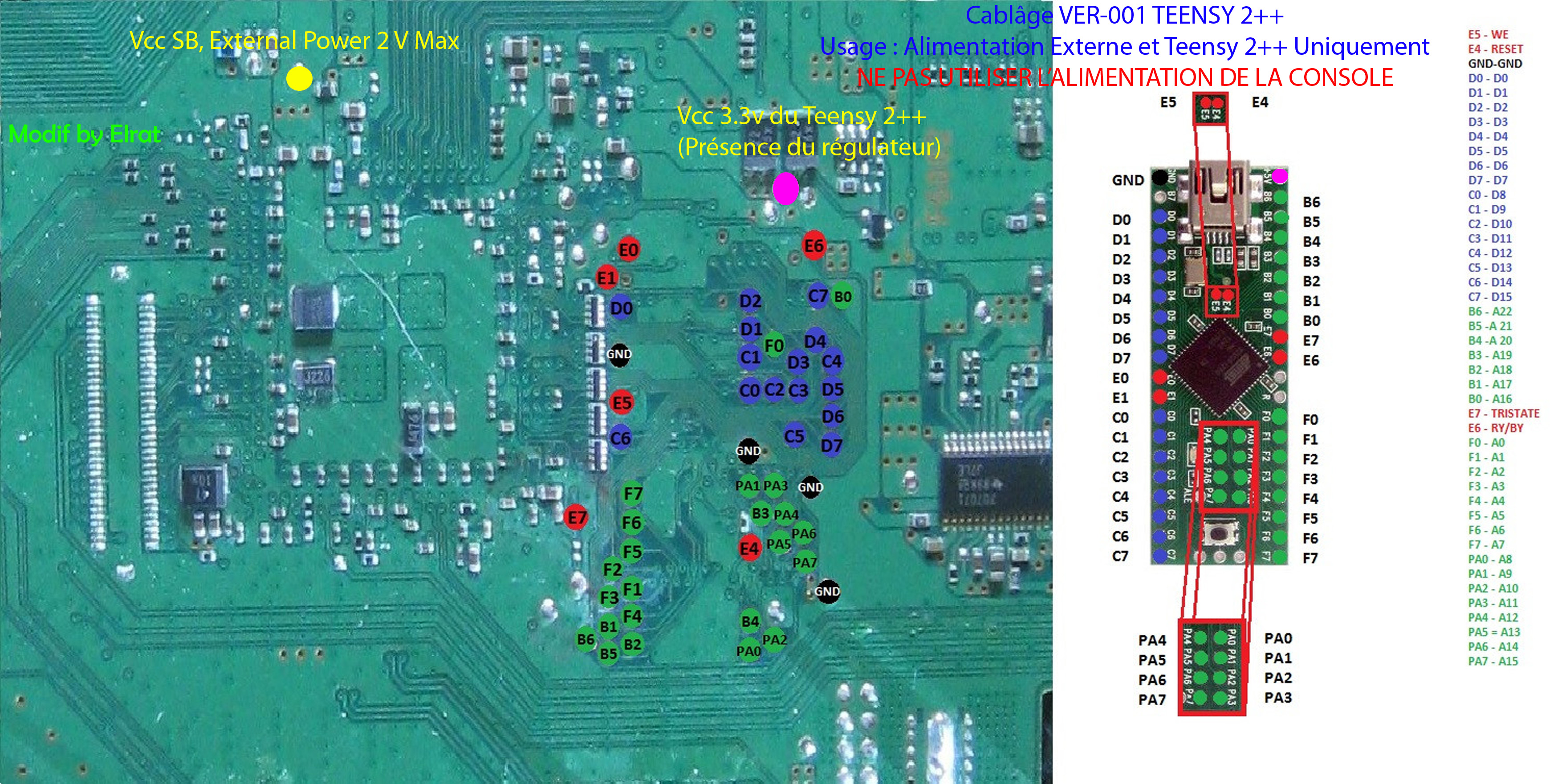
Finding the tristate is another adventure in itself, the purpose of the tristate pin (in southbridge) it to make all the other I/O pins of the southbridge to enter in a special state (named literally tristate... a.k.a "the third state")

The theory is... an I/O pin usually have only 2 states (like an ON/OFF) that represents byte 0 or 1
But sometimes that states could be problematic because we dont want any state... lets say... the state 0 represents something and 1 represents a different something... but we dont want anything, thats the purpose of the tristate
The tristate doesnt represents anything... technically is the same than if we take a solder iron and desolder all the I/O pins of the southbridge from the motherboard
When the tristate is enabled it means that the syscon is not able to communicate with his "peripheral devices" (and are a lot, USB ports, LAN, FLASH, BD, SATA, etc...)
If we try to turn ON the PS3 with the tristate enabled the PS3 cant complete the boot sequence (because is not able to find the peripherals), and it stays quiet in a black screen. But doesnt auto-shutdowns, you have half of the motherboard components "inactive", but is stable

The reason why sometimes is useful to enable the tristate when using a flasher is because we are "disconnecting" southbridge from FLASH, this way our write/read commands from the flasher are not going to have any interference from the southbridge
This way the southbridge is not going to try to read data from FLASH when the PS3 boots

-------------------------
I know some of you already know how this works, im just explaining it in general if there is someone interested in it :)

The way to enable the southbridge tristate is always by connecting the tristate pin to ground, the circuit is designed for it, is safe
But i said it could be dangerous because right now you are not completly sure which tespad is the tristate... lets say... you think you found it but instead of tristate the point you are using is some voltage line... so you solder a wire in between it and ground then you turn ON the PS3 and BOOM the fireworks !

The other pins flash pins are not much problematic, specially the ones for data, if you connect them incorrectly in between the flash and the flasher the most that could happen is that you are going to receive "garbage" when you read it (or more garbage when writing)... in the specific addresss related with that specific wire
But this is not going to cause any damage to the circuits

So is very important to identify the tristate tespad very well before using it (incase of doubts i would not use it)

You only need to use the tristate incase your flasher requires to have the motherboard turned ON btw... in other words, when the power to the FLASH is provided by the PS3 PSU
But... there are some flashers (like teensy) where you are powering the NOR directly with the flasher (so the rest of motherboard components are not powered, we dont need to do the tristate because the southbride is completly inactive)
I dont know your flasher, so im not sure if you need to use the tristate
Btw, are you planning to do this to install a flasher permanently ? (to have an anti-brick setup and to work in CFW development)

--------------------
The tristate pin of the southbridge should be connected always to a testpad... because that testpad is intended to connect with it in factory (or service repair) with a testbench using pogo-pins (i think is named "jig-pin machine" in sony slang)
That testpad for tristate is a "must have" for them when they designs the motherboards, so we know it exists for sure

Aaaaand... im not so sure if the tristate is connected to any other component of the motherboard... the only other component that could potentially be able to do the tristate is the syscon chip... but i dont think it does it
So... i guess the tristate pin of southbridge is not connected to any other component (other than the testpad for the jig-pin machine)
And it should be located very close to the southbridge
 
@sandungas
hehe, I haven't touched her, and patiently waited for your answer. googling such things is not my strength, so many thanks for your detailed explanation. hey, I love most of your answers, because they are so extensive and just "1337" :D

damn, I have to search for tristate, cause I've already bricked with bad coreos :confused:
and yes, this will be a e3flasher permanent install, but no dualboot like on my cechl. I won't cut here anything! now you have mentioned, that teensy can live without tristate, maybe I will get one of these or @littlebalup has mentioned some new programmer, but there is not much info on net, regarding ps3 flashs. have still to think about this and in mean time, I will search and document all pins on my tool.

just remembered, there is some e3mod from bwe, where he externally powers it, so I will also take a look at this one

btw, do you know the codename of a 1400A? it is DEB-001, so is it maybe a "DEBORAH"? or more like "DEBRIS" for the frankenstein components?

anyways, here some pix of my 'personal graveyard', lol

so it is a 4000er superslim first, then slim (I think it was 2504, dunno anymore), my rsod cechl (this has suddenly stopped working, so I should have replaced nor), my broken ylod cechl, a ylod cechc and last but not least my baby. can you see those dark traces on the deb-001? besides, all components look somehow cleaner and perfectly aligned. on the others you can find a few crooked components, but not on her!

have located tristate on southbridge pins, with removed southbridge on my cechl
it is located upside. I know there should be somewhere some additional tristate next to southbridge. you can find more details on psxtools. will take it as some 'blueprint'
 
Last edited:
Lol @ DEBORAH and DEBRIS, i dont know the real codename but that ones would be funny, the other names they used as COOKIE and VERTIGO sounds a bit funny to me too (because doesnt sounds much serious, i could never imagined by myself, lol)

i cant see your images, for some reason are very tiny when i try to click in them, the best images of a DEB-001 i found are this ones:
https://www.psdevwiki.com/ps3/DEB-001
And the testpads are over here:
12VwDnY.jpg


The white circle at left is where tristate should be located... im marking this area because the southbridge is at the other side, so is one of the "big" testpads that can be seen in there, almost for sure
As i mentioned before is pointless to locate the tristate far away from the southbridge, so it needs to be very close to it... but in the "bottom side" of the motherboard im marking because the "jig-pin machine" is attached to the back of the motherboard
The southbridge of the DEB-001 is exactly the same than in VER_001 btw (CXD2984AGB) https://www.psdevwiki.com/ps3/South_Bridge#Chipnumbers_.40_SKU.27s
So... we need to try to see where is located the tristate testpad in VER-001 and compare the circuit/traces/components around it and see if it looks the same in DEB-001

And the circle i marked at right... well... thats obviouslly the testpads to program the NOR chip
I been taking a look at the photos for retail motherboards here:
https://www.psdevwiki.com/ps3/Motherboard_Revisions
And the "flash testpad layouts" images here:
https://www.psdevwiki.com/ps3/Teensy++_2.0#Schematics_by_motherboard

But i cant find any where the flash testpads looks like the DEB-001... im not sure if im missing something, this requires to continue comparing more photos, im not completly sure if the location of the flash testpads in DEB-001 is "unique"
 
Hmmm, in this image it can be seen where is located the tristate testpad in VER-001 (marked as "E7")
Sadly the motherboard was very dirty in that area so we cant appreciate the traces around it :/
VER-001_TEENSY_External_Power.jpg


And we dont have any other good photo of a VER-011 to try to see how this small area of the circuit looks
https://www.psdevwiki.com/ps3/VER-00x

But... i can see they "displaced" the tristate testpad a bit in the direction of the other flash testpads, see where is located the testpad marked as "E7" in the VER-001
So... maybe in DEB-001 is closer to the others too, there are a couple of candidates i marked in blue, it could be like this
2mM5g6T.jpg
 
I mean... the logic im following is this:

1) the southbridge of VER-001 and DEB-001 is exactly the same... so the traces and other components around it should be pretty much the same, and even his positions
2) In VER-001 the tristate testpad is located in a corner of the southbridge... so in DEB-001 should be located pretty much in the same corner

The result is this, there are only 2 posible candidates ;)
The square is your shouthbridge and the arrow indicates the 2 posible testpad candidates at his corner
FBXwbLT.png


Edit:
And one of the testpads i said that could be a candidate seems to be GND (is hard to tell, the photo is not good enought)... so the tristate should be the other (where the arrow points)... so i think i got it :D


Edit2:
Btw, please check and re-check all the images from VER-001 and your DEB-001 to see if the southbridge in DEB-001 is "rotated" when compared with VER-001
I dont think is rotated, but this is a detail i didnt checked... is very important to be sure where is located the corner with the tristate pin
 
Last edited:
@sandungas
jup, just wanted to upload a picture. this is exactly what I am thinking, now I have compared cechl to decr
to verify, I will use "trick17", as we german call it, and use a thin copper wire and place it in the same area on the decr soutbridge. if I am lucky, the testpoint is also located at the exact same spot under southbridge, pin 6 from left on top, as highlighted in my picture. to get the probe better "stickied", I will solder some blop on the suspected testpoint :)

oh, and thanks again for your help here. I/we really appreciate it

btw, I have located now all gnd/vss points. now comes the hard part to find and numerate all other points

erm wait, about the other points, are they also dangerous if misplaced or is tristate the only one? well, nvm. the others are all located on the nor chip itself, puh

about the pictures, I will edit the posts to make them more visible. but somehow, the 1st picture was edited by a mod, cause of size. at least I was noticed with this message
 
Last edited:
I been reviewing the photos of all retail motherboards (and some non-retail too) and i think the layout of the flash testpoints for DEB-001 are really unique :/
It surprises me a bit because they could "recycle" that area of the circuit design from one of the retails fats, this would reduce a bit the costs of designing and building the adapter for the "jig-pin machine"
But nah... the design of the circuit is completly new

Also, i realized why is so different, the last retail motherboard for fats is the VER-001 and have the serial number 1-878-196-xx
And the serial number of DEB-001 is 1-879-845-xx (a bigger number, so is newer)
So the DEB-001 is the last revision of the PS3 fats motherboards
Actually... chronologically is located in between the PS3 fats and the PS3 slims :D

-----------------
Btw, try to identify the 5 "control" signals, are the most important and should not be specially confusing
-CE (chip enable)
-OE (output enable)
-WE (write enable)
-RB (ready/busy)
-RESET
 
Also, i realized why is so different, the last retail motherboard for fats is the VER-001 and have the serial number 1-878-196-xx
And the serial number of DEB-001 is 1-879-845-xx (a bigger number, so is newer)
So the DEB-001 is the last revision of the PS3 fats motherboards
Actually... chronologically is located in between the PS3 fats and the PS3 slims :D
this is what I have also suspected, that it was the last of fat nors, but somehow they have chosen the mainboard design from a cechc-cechh (a/b should also be similar) and not the one used for ver-001

-----------------
Btw, try to identify the 5 "control" signals, are the most important and should not be specially confusing
-CE (chip enable)
-OE (output enable)
-WE (write enable)
-RB (ready/busy)
-RESET
I will test them chronologically, one after another. unfortunately, they are not straight aligned like on a ver-001
 
erm wait, about the other points, are they also dangerous if misplaced or is tristate the only one? well, nvm. the others are all located on the nor chip itself, puh
Are tricky to find because the posture of your body is uncomfortable, you need to touch with a probe of the multimeter in a side of the motherboard, and the other probe at the other side, if you have someone to help you (to grab the motherboard vertically while you move the hands around it) thats a nice help
Otherway if you want to do it alone... what i use to do is to seat in a chair, then i place a towell in my legs, and the motherboard vertically in between the legs (i use the legs a bit to grab it, lol), this way i have the hands free to move them around :D

You need to touch one pin of the NOR chip in a side of the motherboard, then touch all the other testpads in the other side (are a lot and only one of them is the winner that is going to make the multimeter to "beep")

As said... try to find the 5 control pins first... after that (and the tristate, volts, and gnd that seems you already found).. all the others are data
There are 32 pins for data... let them for the ending... are the most boring because you need to repeat the same 32 times

The most dangerous are tristate, volts and ground, because thats where you could create a shortcircuit by mistake later (not now because now you dont have electricity in the motherboard)
about the pictures, I will edit the posts to make them more visible. but somehow, the 1st picture was edited by a mod, cause of size. at least I was noticed with this message
It was me the other day sorry, i was trying to "fix" the image because was not displayed fine, but after i edited your post the image was not displayed fine anyway, so i stopped messing around with your post (i failed at fixing it, oppps)
Better upload the images to https://imgur.com/upload?nc=1 (open the link and drag and drop)
Or attach them to the forum in your post
 
Last edited:
@sandungas
damnit, luck disappears :(

#OE and #CE are both grounded. how to solve this issue? maybe my intuition helps here...

and thanks for the link. I will reupload my pictures there then

I am using your same technique to probe them, since I am all alone (we was pointed to my DEBORAH, lol). this is why I solder blops on the testpoints to get the probe better stickied, so I can move on the chip freely
 
Last edited:
#OE and #CE are both grounded. how to solve this issue? maybe my intuition helps here...
Im checking #OE and #CE in a JSD-001 motherboard, the multimeter does a "beep" when checking continuity in between them and ground, but if i configure the multimeter to meassure resistance the display indicates 670ohm
The multimeter is beeping because the resistance is low, but are not connected directly to ground

Most of the other testpads displays the same resistance to ground btw
 
I had trouble finding the tri-state point on my ver 00 that I permanently installed an e3 flasher in. I documented it over in the hardware mods section. I think the thread was called my e3 flasher journey or something. I remember having to remove a small resistor and soldering to one of the legs to initiate tri-state and dual boot. Been awhile, I got it wrong the first time, then figured it out with the help kp420, and Lilballup in the end.
 

Similar threads

Back
Top