PS3 PS3 CECHC04 console, NAND memory chip problem

zsolt94

Forum Noob
Hi everyone,

I am an avid PS3 FAT BC collector and I bought a console that doesn't work. Model CECHC04, with a COK-002 motherboard.
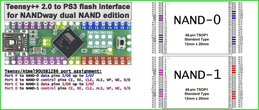
I took it apart and wanted to read Syscon error codes and make dumps of the contents of the NAND0 and NAND1 chips with a hardware flasher. (TEENSY and NANDway)
NAND0 is fully readable, but NAND1 is unfortunately physically damaged. It's practically broken in two...

Is there any chance that we can restore the contents of the NAND1 chip based on the NAND0 dump?
Let's say based on the NAND0 and NAND1 dumps of another working console?

Or is the motherboard almost beyond repair with this defect?

Any help would be greatly appreciated,
 
Unfortunately, I do not think there is a straightforward way to rebuild a completely missing NAND1 from NAND0 alone.
On these PS3 NAND models, the two NAND chips are interleaved into one logical flash image. In practical terms, that means the data is split across both chips, so if one NAND is physically destroyed, part of the total flash is gone with it. Because of that, you generally cannot reconstruct the missing chip from only the surviving one. PS3 flashing guides and dump-validation resources treat the two NANDs as a pair that must be combined/interleaved to produce a valid unified dump, and they warn that without proper dumps you can end up with an unrecoverable flash.

Using NAND0 from your console and NAND1 from another working donor console is also very unlikely to work as a direct fix. Even if the layout looks similar, there is console-specific data in the flash, so mixing halves from two different boards would almost certainly create an invalid image. I have never seen that used as a reliable recovery method. That said, as an experiment, it could still be interesting to interleave a donor pair and study the extracted structure just to better understand how the data is distributed. The interleave/de-interleave workflow itself is well documented in the PS3 scene tools, but that is not the same thing as true reconstruction of a missing chip.

The only possible workaround I can think of would be a true hardware-level recovery attempt on the damaged NAND1 itself. In other fields, people do sometimes grind into damaged NAND packages and manually recover connections from the die/package traces, but that is extremely specialized work, very difficult, and usually only done for high-value data recovery cases. If the chip is physically cracked badly enough, even that may not be realistic. I have done this on iPhone Nands and even SD cards....

So in my opinion, your options are basically:
  1. Try to recover the original NAND1 physically, if the damage is limited and you have the tools/skill for advanced chip recovery.
  2. Treat the motherboard as a parts board if NAND1 is too badly damaged.
  3. As a research project, experiment with donor dumps only to study structure/interleaving, but not with much expectation of producing a bootable repair.
In short: if NAND1 is truly broken beyond readout, the board is probably very close to beyond practical repair.


Thank you very much for your answer.

Somehow I had a feeling that this would be a very difficult task.
Anyway, I'll read up on chip data recovery. I'll also need to buy a good quality microscope.

As I see it, there shouldn't be many connections (approx. 15 pcs pin) to recover the data if the chip itself isn't damaged inside the casing.
Source: https://www.psdevwiki.com/ps3/Teensy++_2.0
850px-Teensy%2B%2B_2.0_to_PS3_flash_interface_for_NANDway_dual_NAND_edition.jpg


The NAND1 chip is visually in this condition: (someone treated it badly...)
upload_2026-3-19_21-1-10.png


In the worst case, this will be my practice board where I can try BGA soldering.
One day I'd like to make my own 40nm RSX Frankie mod :D
 
Its a shame my budy at the data lab has a laser that will litterally remove all the casing on that chip and expos the pads/traces haha but in a pinch a good IC Polishing Grinder Pen for iPhone Touch IC chip removal or Memory Polishing can prolly get it done that chip style is very old i mean i do chips that are new age right ya feel me :)

YA man i mean take a good one NAND and pratice cause youll have to know feel for depth and a few things then when ya got both sides of crack polished down and exposed fly wire em with 40 or 50 guage wire hahah its fun stuff man pain in the but ya you will 100% need a high grade microscope that is a fact!

Good luck dude~

One thought dont remove that fromt he board solder the wires to the legs and put presurre on that chip maybe you could be lucky and even though its cracked traces that are requried maybe still intack??? worth a shot befor ya start polishing away the case
 
Last edited by a moderator:
Back
Top