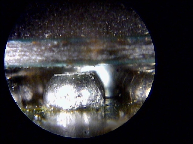
I just want people to see this, because when we talk about BGA "defects" people envision cracks. More often it looks like this...
The greatest tension forces are on the edge of the BGA. That's where the majority of the VDDIO and FlexIO lines are connected, which explains why they are the most common errors we see (when the BGA is actuall at fault. Bumpgate claims the rest).
The bond with the Copper pad is important to prevent this type of BGA failure. Yes a crack can occur, if the bond with the pads are strong enough to hold and actually deform the solderball (literally squash and pull it). In that case, yes you can form a solder "crack" over time. But that's not the most common type of failure, it's the one in the picture.
The ball litterally pulls away from the pad, or tears the pad off the board! That's due to imperfect reflow profiles, flux, contamination on the pad, solder chemistry, the ahesive used to ahdeare the pad to the FR4 interposer/substrate, even the adherance method used when placing the chip (modern BGA machines actually hover the chip over the pads until the balls go molten and then place them down).
Often what you see when you remove a GPU are dull or black pads. That because when this fault occurs, it exposes the copper pad to the air, which contain oxygen. Oxygen oxidizes. That's why you have to use flux, to prevent oxygen from coming into contact with the surfaces you're welding. The problem is that these pads are usually exposed for a long time before the reflow is performed. So the pads have a thick layer of oxides built up on the pad. Solder wont stick to the oxide layer. And flux doesn't remove it that well.
That's why reflows usually don't work. And if they do, they don't for long. It's why reballing is necessary. So you can literally scrape the oxide layer off and get shiny pads for a lasting bond. And the quality of the reballed bond is highly dependent upon the skill of the technition and equipment used.
")


