Looks good, thanks for this. Will probably replacing mine with these in the guide.
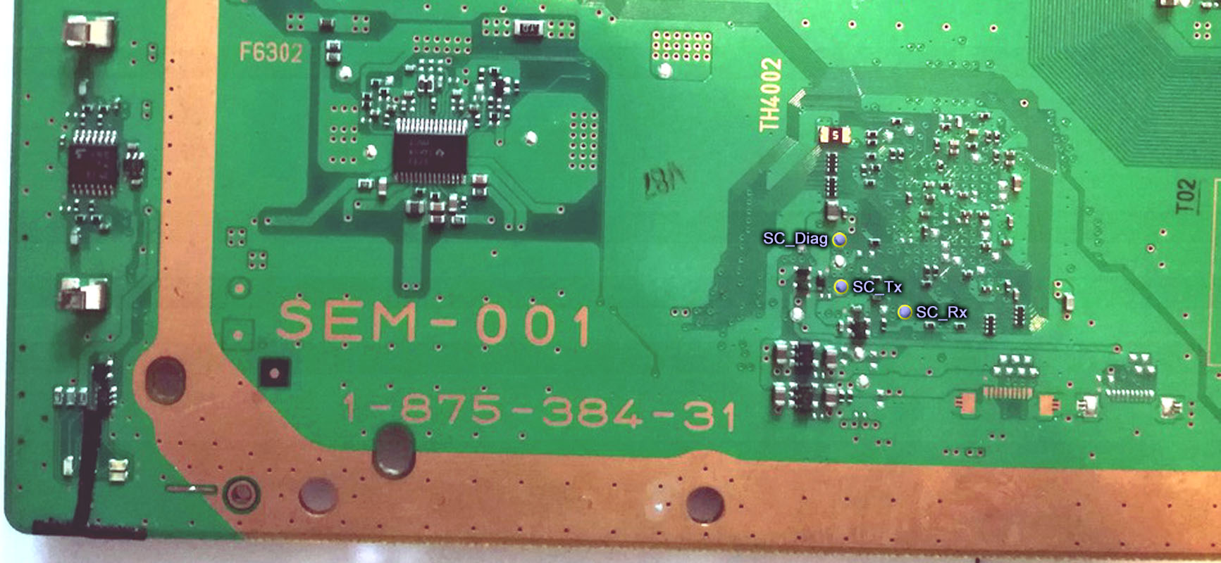
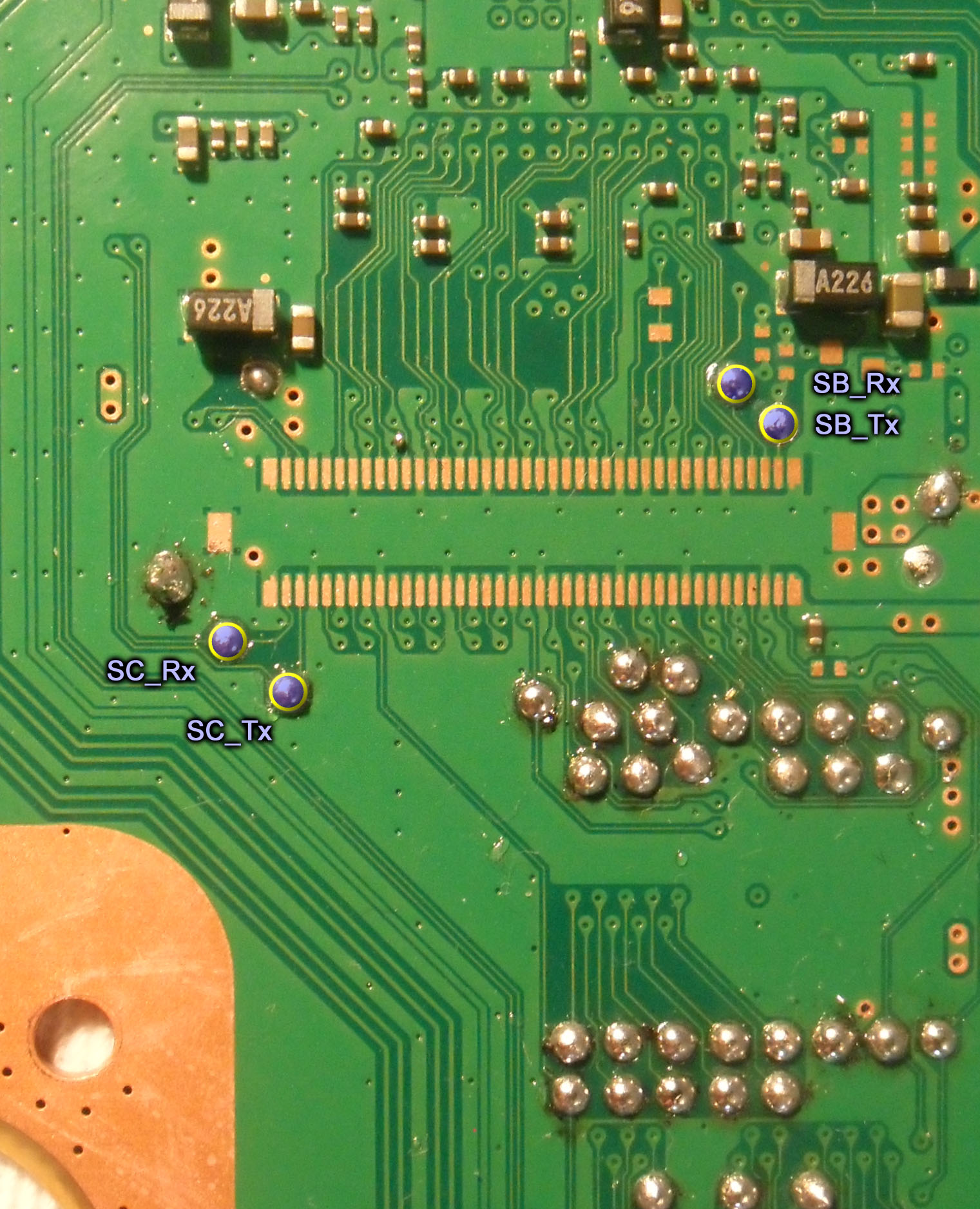
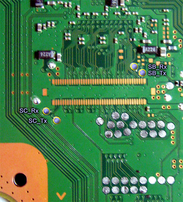
See you have the Southbridge Uart pins aswell, just need to add the COK-001,002 and SEM-001 SB pin outs. The SEM-001 SB pins need a 0.1 ohm resistors to connect to the pins.
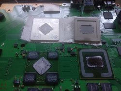
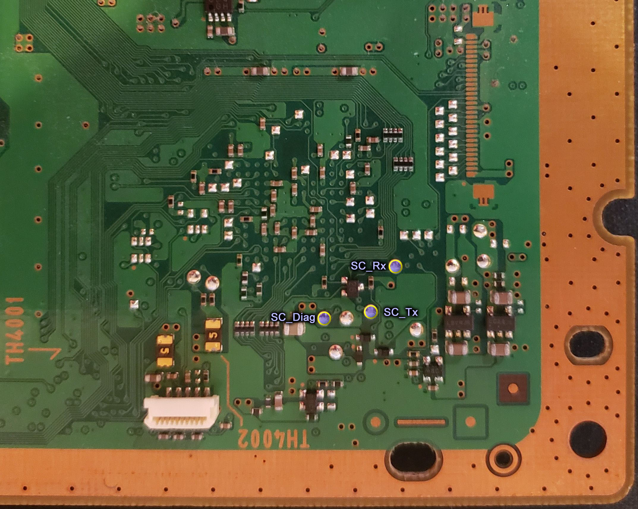
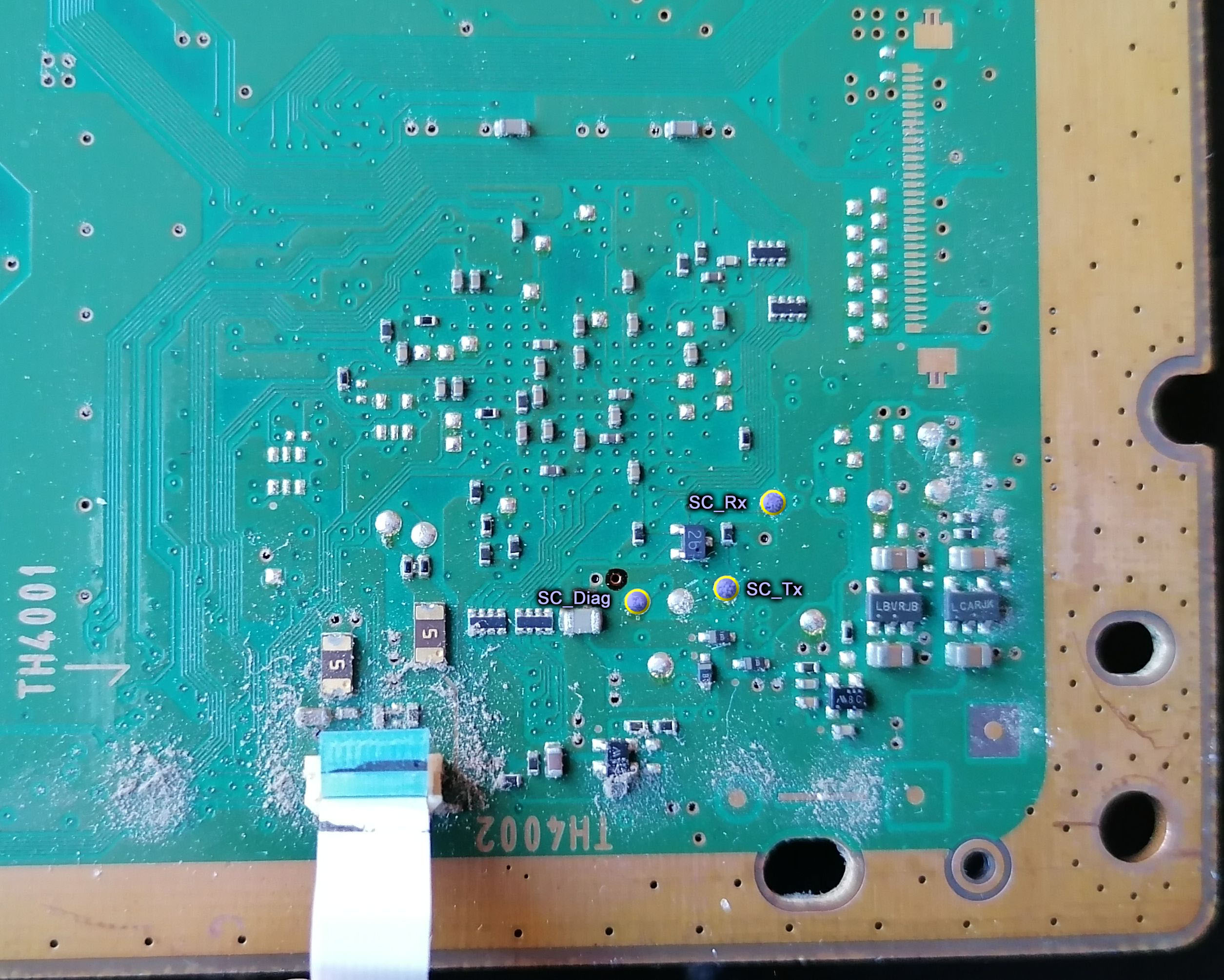
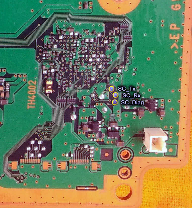
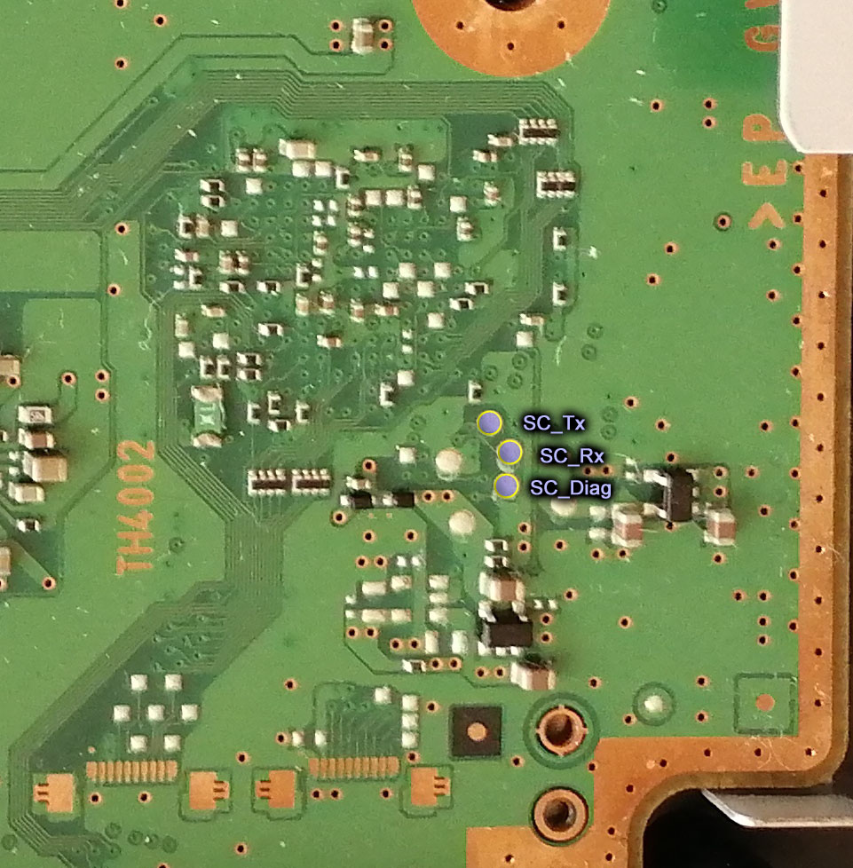
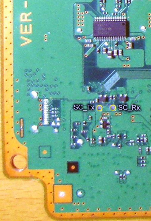
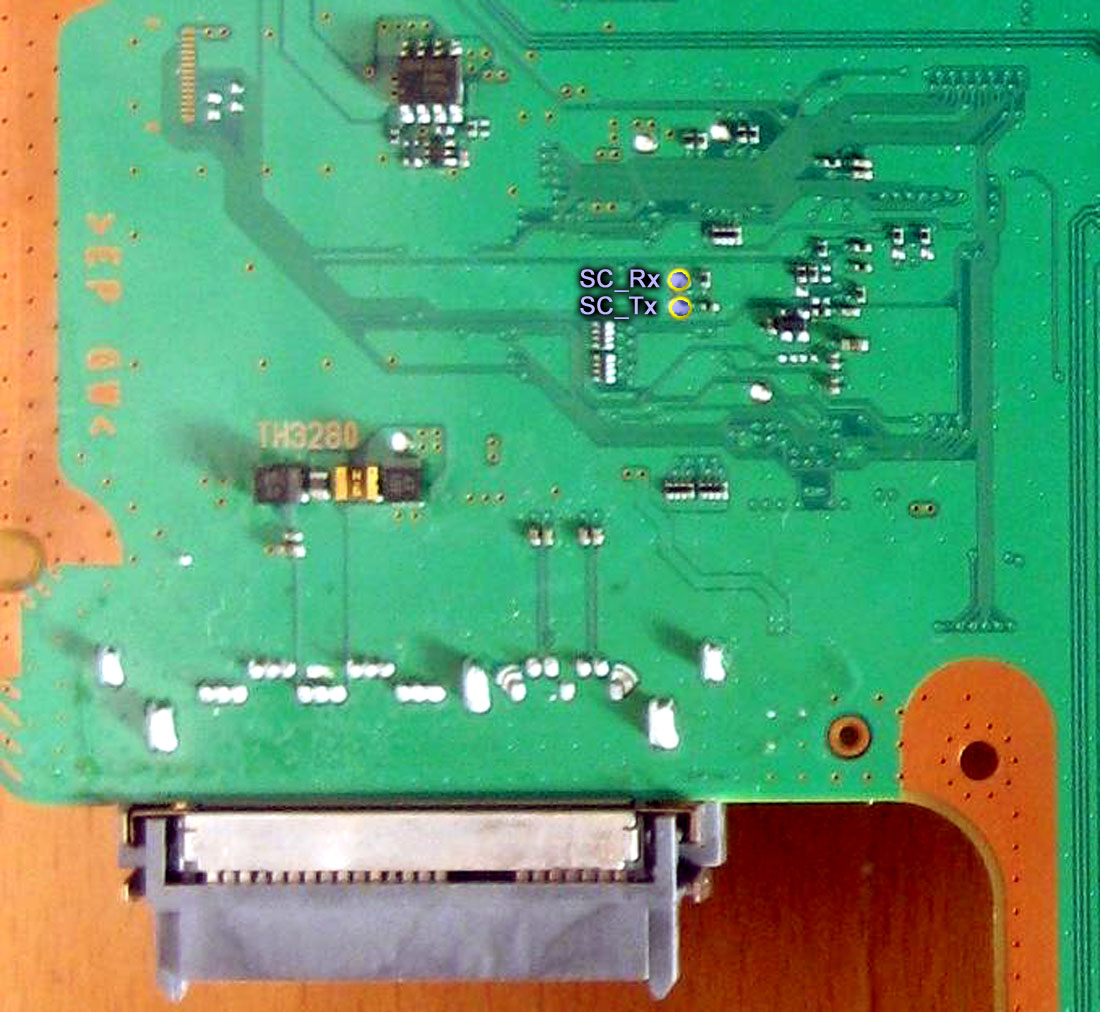
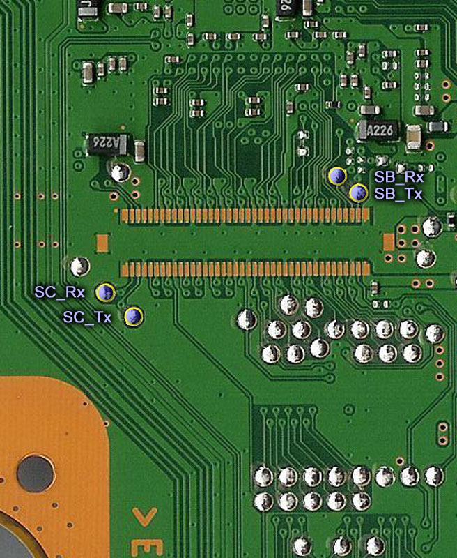
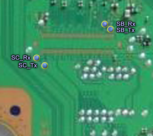
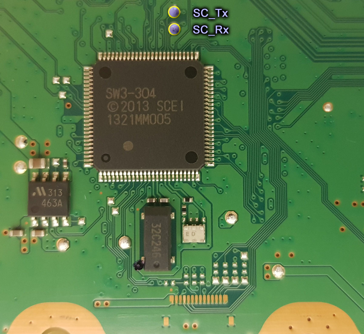
I added the SB UART testpads only in the images from layout 6 (SUR-001, JTP-001, JSD-001, KTE-001) because are very close to the SC UART testpads so it was convenient to have both in the same image, also i was confident because we was discussing them before
here
That long dual-line of solder pads in the images from layout 6 (SUR-001, JTP-001, JSD-001, KTE-001) is the PCI connector. In most of the other images for other motherboards appears
the service connector/s and that service connectors handles the SB UART too
The problem is... if the SB UART testpads are located in the images i uploaded, please "paint" on top of them to indicate it to me and i will update the image in wiki
Otherway... if the SB UART tespads are located far away (in other words, outside of the images i uploaded) then we have a problem because it took me lot of time to find some of that images in google (in wiki we dont have good quality photos of a lot of the PS3 motherboards). With this i mean... i cant "expand" the image to show a bigger motherboard area. Also if the SB UART tespads are located far away from the SC UART testpads is better to make 2 different images for them
Btw, as curiosity sake, for alternative solder ponts... in the images where can be seen the service connectors the solder pads of the SB UART pins of that service connector is mapped in wiki
As example... if we take the photo i uploaded of the COK-001... the (unpopulated) service connector is at top-right corner, and the pins needs to be counted "from bottom to top"
Then compare with
this pinout of the CN4009
Are pins #18 and #19 of the service connector. In other words... are the 2 lines that goes to the left, then dissapears out of the photo in diagonal north-west direction
Long story short... i dont know where are located the SB UART testpads of the other motherboard models, if can be added to the photos i uploaded advise me and i will update them in wiki
Incase cant be added to the photos i uploded we need to make another collection with different images