PS3 Fault finding YLOD with the SYSCON - First steps and Error reporting

I added the SB UART testpads only in the images from layout 6 (SUR-001, JTP-001, JSD-001, KTE-001) because are very close to the SC UART testpads so it was convenient to have both in the same image, also i was confident because we was discussing them before here

That long dual-line of solder pads in the images from layout 6 (SUR-001, JTP-001, JSD-001, KTE-001) is the PCI connector. In most of the other images for other motherboards appears the service connector/s and that service connectors handles the SB UART too

The problem is... if the SB UART testpads are located in the images i uploaded, please "paint" on top of them to indicate it to me and i will update the image in wiki
Otherway... if the SB UART tespads are located far away (in other words, outside of the images i uploaded) then we have a problem because it took me lot of time to find some of that images in google (in wiki we dont have good quality photos of a lot of the PS3 motherboards). With this i mean... i cant "expand" the image to show a bigger motherboard area. Also if the SB UART tespads are located far away from the SC UART testpads is better to make 2 different images for them

Btw, as curiosity sake, for alternative solder ponts... in the images where can be seen the service connectors the solder pads of the SB UART pins of that service connector is mapped in wiki
As example... if we take the photo i uploaded of the COK-001... the (unpopulated) service connector is at top-right corner, and the pins needs to be counted "from bottom to top"
Then compare with this pinout of the CN4009
Are pins #18 and #19 of the service connector. In other words... are the 2 lines that goes to the left, then dissapears out of the photo in diagonal north-west direction


Long story short... i dont know where are located the SB UART testpads of the other motherboard models, if can be added to the photos i uploaded advise me and i will update them in wiki
Incase cant be added to the photos i uploded we need to make another collection with different images
Got your point, you can simply solder wires to enable that port 18,19 pins is very easy I will add/edit some photos, never known who is Rx, Tx (easy find by swap.
Anyway both SDA/SCL are interconect in parallel from both cpu/rsx and going to syscon on a single port .Only a single line have a 50 ohms resistor, not sure which. This is what I'm working.
After reball still 2130 and can't find issue, I will pm flash dump if you are interested,
Both tmp0/1 are fine after 30 minutes stable. Now thinking only to change rsx tmp ic only it was last, but also I think for last experimental, swap to another donnor board.
It also can be dead rsx...
Have to wait for cpu silicone to get cured, will see after more tests.
Will run further tests in time, as this becomes a pain.
This is from cok002
c5a3cc33fac766f7e728f130eed44721.jpg
Edit
Just don't forget to edit details on devwiki
12cd51629198935fe82160417429db8b.jpg
850c0f049778d31c89e2a7cd35c30161.jpg
a813b3b75d39210b863de45251b86a91.jpg
About this dyn001 board with 2130 is something that can't be done quickly so for the moment can wait.
 
Last edited:
Got your point, you can simply solder wires to enable that port 18,19 pins is very easy I will add/edit some photos, never known who is Rx, Tx (easy find by swap.
Anyway both SDA/SCL are interconect in parallel from both cpu/rsx and going to syscon on a single port .Only a single line have a 50 ohms resistor, not sure which. This is what I'm working.
After reball still 2130 and can't find issue, I will pm flash dump if you are interested,
Both tmp0/1 are fine after 30 minutes stable. Now thinking only to change rsx tmp ic only it was last, but also I think for last experimental, swap to another donnor board.
It also can be dead rsx...
Have to wait for cpu silicone to get cured, will see after more tests.
Will run further tests in time, as this becomes a pain.
c5a3cc33fac766f7e728f130eed44721.jpg
Edit
Just don't forget to edit details on devwiki
12cd51629198935fe82160417429db8b.jpg
850c0f049778d31c89e2a7cd35c30161.jpg
a813b3b75d39210b863de45251b86a91.jpg
About this dyn001 board with 2130 is something that can't be done quickly so for the moment can wait.
Thats the point... if the pinout of the service connector is mapped in wiki (and all them are, at least for SC and SB UART lines) we can find the SB UART testpads (the big ones, intended to connect the pogo-pin machine). The same can be made in all PS3 models... like a bloodhound dog following the lines starting from the service connector :)

The most handy are the testpads because is easyer to solder in them so everybody is going to be more interested in having a photo of them, and are not going to be interested in the pinout of the service connector, but when i was cropping the images (trying to include something as reference) i realized in lot of them the service connector was very close, so i included it in the image, as reference but also because is completly related, and well... eventually the images i uploaded can be updated to add some info about that pins of the service connectors

And yeah... incase of doing the UART connections in the service connector pins, is needed either to restore the original components (but are unkown, probably resistors or diodes to protect the lines), or to "bridge" some pads located at intermediate points of the lines, in the way you marked them in your photo of the COK-002 (there are 2 more not marked in your photo, in between the PCI pins and the tespads), if we want to complete this collection of "bridges" to restore the lines of the service connectors are going to be needed lot of photos

-----------
The SDA/SCL in between syscon and the thermal monitor chips is the "2 wires" data bus i was mentioning, in the datasheet of the TMP411 is mentioned literally that it uses the "SMbus" protocol
The specific wiki pages for the sherwood syscons (and some of the info related with sherwoods in other pages) is a bit messy, are in progress of being updated, probably in the next days/weeks
One of the problems is... if you click here in the specific pages of each sherwood syscon you are going to see everyone have a different pinout table, this has been an annoyance since many time ago because we was not sure how many syscon models was sharing the same pinout, but now it seems there are only 3 pinouts, based in the package type:
1) BGA 200 pads = for all the mullions (the specific wiki pages has been updated and all them shows the same template)
2) QFP 128 pins (the rectangled syscons) = Used by Sherwoods SW & SW2 series ---> by now only is shown in this page
3) QFP 100 pins (the squared syscons) = Used by SW3 series Sherwoods (this ones only have a few pins mapped)

I think the data sent in between syscon and the thermal monitors throught the SMbus contains the configuration, i mean... inmediatly when we power the PS3 syscon does an "initialization" of the thermal monitor chips by sending his configuration... and after that the thermal monitors sends data to syscon that only contains the "actual temperature"
That initial communication contianing the config data could be very interesting because we could use it to figure how syscon is configuring them... i mean... with a huge work reverse engineering the syscon firmware maybe someone will be able to figure it... but having that data could help a lot because it would allow that same person to "walk backwards" to try to see how the syscon is generating that data
As i said before, it must be composed by some values that are hardcoded (because is pointless to change them, the engineers working with the prototype PS3 never needed to change them and we dont need to change it either), some more that probably can be configured and are located in regions intended to be modifyed (the "Platform config", or "Board config", the "thermal config", or regions like that availables to be modifyed by us with the basic UART acces we have now. In other words... probably some of that settings are located in areas we can read/write, if we find how it works and (if we are lucky) we find that we can configure it could be handy for some hacks
By now im not sure how much of it can be configured, but it looks some of the settings inside the "thermal config" area are used to generate that configuration

------
The bewitched DYN-001 only shows error 2130 now ?, and the termperatures you see by UART are aceptable (looks realistic) ?, i guess this means the CELL thermal monitor chip was bad ?, because you reoplaced it, right ?
Have you replaced the 2 capacitors and 2 resitors around the CELL thermal monitor chip ?... as i mentioned before, this ones are the last components related with this subcircuit, there is nothing more that could be the culprit... except the CELL internals

What you did with the CELL ?, i guess is the same one, right ?, keep in mind whatever that damaged the thermal monitor chip (that seems it was damaged and now is working fine) happened at the same time the error 2130 you are having now
Actually, at some point you said you noticed some marks in the thermal monitor chip... so the previous person that was trying to fix it maybe damaged the thermal monitor chip... and the thermal sensor inside CELL too

Dunno, but to me it looks the CELL sensor is damaged, so the "gheto fix" i mentioned the other day by adding a custom sensor to the thermal monitor chip comes in mind again
And btw... i remember months ago there was someone in the forum reporting temperature value 255ºC in webman with a screenshot as a proof (but obviouslly it was not realistic). The point is... the thermal monitor chip was damaged, but the PS3 was booting fine into XMB and working normally (probably syscon was throwing internal errors but it seems it was booting anyway)
So... try to mimick that behaviour... boot without the thermal monitor chip... or take the damaged thermal monitor chip and solder it to the motherboard without pins #2 and #3 (this way is not connected to CELL at all)

Or just try to install a PS3 firmware, maybe the fact you are seeeing a 2130 in syscon UART doesnt matters much and is going to allow to install it
 
Last edited:
Ok about this dyn001 is the same with 1200, 2130. After exchange of tmp A ic for cpu, error 1200 disappeared, left only 2130. Reballed both didn't change. Flashing nor reversed and back to normal didn't change anything.
Now remember I've seen traces on rsx tmp ic as someone previously thought is an eprom thinking to read it(it seems like that) . Now because they work in parallel I assume syscon does not know exactly which Id is broken because of simultan data is received but not sure if A or B id is partially correct.
Not sure how it work for debugging always wasn't very clear and that's why I tend to believe more on hardware testing.
Now what's left exchange B (rsx tmp ic), test getto mod, port cpu(all his parts) to a donnor working board (have one with artefacts on XMB, think to exchange nec's for experimental as last resort )
>$ auth
Auth1 response invalid
>$ auth
Auth successful
>$ errlog
00000000
# CODE CLOCK
# A0112130 FFFFFFFF
# A0112130 FFFFFFFF
# A0102130 FFFFFFFF
# A0A02130 FFFFFFFF
# A0A02130 FFFFFFFF
# A0111200 FFFFFFFF
# A0112130 FFFFFFFF
# A0112130 FFFFFFFF
# A0112130 FFFFFFFF
# A0092130 FFFFFFFF
# A0112130 FFFFFFFF
# A0092130 FFFFFFFF
# FFFFFFFF FFFFFFFF
# FFFFFFFF FFFFFFFF
# FFFFFFFF FFFFFFFF
# FFFFFFFF FFFFFFFF
# FFFFFFFF FFFFFFFF
# FFFFFFFF FFFFFFFF
# FFFFFFFF FFFFFFFF
# FFFFFFFF FFFFFFFF
# FFFFFFFF FFFFFFFF
# FFFFFFFF FFFFFFFF
# FFFFFFFF FFFFFFFF
# FFFFFFFF FFFFFFFF
# FFFFFFFF FFFFFFFF
# FFFFFFFF FFFFFFFF
# FFFFFFFF FFFFFFFF
# FFFFFFFF FFFFFFFF
# FFFFFFFF FFFFFFFF
# FFFFFFFF FFFFFFFF
# FFFFFFFF FFFFFFFF
>$ tmp 0
00000000
# TZone No:00
# Temperature:+52.75(0x34C3)
>$ tmp 1
00000000
# TZone No:01
# Temperature:+49.0(0x3100)
>$ csum
F0000006
>$ tmp 0
00000000
# TZone No:00
# Temperature:+54.0(0x3603)
>$ tmp 1
00000000
# TZone No:01
# Temperature:+50.75(0x32C0)
>$ version
00000000
# Sherwood Version = 1.11.0
>$ tmp 0
00000000
# TZone No:00
# Temperature:+54.75(0x36C3)
>$ tmp 1
00000000
# TZone No:01
# Temperature:+51.75(0x33C0)
>$ tmp 1
00000000
# TZone No:01
# Temperature:+51.50(0x3380)
>$ tmp 0
00000000
# TZone No:00
# Temperature:+54.25(0x3643)
>$ task
F0000003
# [UCMD] Unknown command.
>$ powupcause
00000000
# Powup Cause: 00 00 00 00 00 00 00 04 00 00 00 00 00 00 00 00
>$ meminfo
F0000003
# [UCMD] Unknown command.
>$ bestat
00000000
# (PowerOn State)
# State = 05
>$ shutdown
00000000
# [SSM] Shutdown Start.
# [SSM] Shutdown ok.
# (PowerOff State)
6e2394b8b31c855588a6584131f036b8.jpg

For cok002 it can be bridge of soldering on those points yellow and red where they are missing under SB I've posted lines.
So what is going to pci it should be a 0 ohms R3209, R3208 to enable pins on PCI port as well.
1c2923106bec12f362067441430ae41d.jpg
 
Last edited:
@vyktormvmpay25 but start with the easyest thing first, have you checked all this ?
1) remove/replace the capacitor in between D+ and D-
2) remove/replace the resistors in D+ and D-
3) remove/replace the capacitor in V
4) replace the voltage regulator that feeds the 2 thermal monitors (i dont know where is located though)

--------
Yeah, that 2 resistors R3209, R3208 in the COK-002 is what i meant (not marked in your image), the service manual tells that are 0 ohms ?. Can you check in the service manual if the other 2 resistors you marked in your photo are 0 ohms too ?
So... in total are 4 resistors of 0 ohms ?
Then i guess the same rule applyes to the SC UART lines to the service connector

In the testpads Layout 6 (SUR-001, JTP-001, JSD-001, KTE-001) are a bunch
The 3 missing components very close to the connector, in this photo
Service_connector_3rd_gen_VERTIGO.jpg

After that the lines goes into VIAS (holes), and appears at the other side of the motherboard, convenienty aligned to a hole in the metal shield, next to the connector of the antennas
Is neeed to fix the 4 missing components here
SC_Serv_Connector.JPG

And finally... 2 more, located very close to the SB_Tx and SB_Rx testpads (on top of them in this photo)
SUR-001_SC_and_SB_UART_testpads.jpg
Ok in sem001 schematic is a proof of concept where some resistance are simply wires/shorted traces. Going to prove with right printscreen if necessary.
On pin 43 and pin 21 if short is added you trace SB-rxtx. So it will lead SB rxtx out to the fpc connector unpopulated on bottom. Been already tested yesterday and was about to update.
 
Last edited:
@db260179 @Pacorretaco @vyktormvmpay25 @RIP-Felix etc...
The other day i made some images of the syscon UART testpads and uploaded them to wiki here

Are intended to have the best quality posible, from photos taken from vertical, i included something as reference (usually a corner of the motherboard), i included also the (unpopulated) service connector if possible, all are made with the same style, etc...
Of course you can use them for tutorials or whatever, if made later in the future check the page in wiki because eventually could be replaced by better versions, there are a couple that are "just meh" but i included them to complete the collection, are 12 in total

Layout 1 (COK-001, COK-002)
COK-001_SC_UART_testpads.jpg

COK-002_SC_UART_testpads.jpg

Layout 2 (SEM-001)
SEM-001_SC_UART_testpads.jpg

Layout 3 (DIA-001, DIA-002)
DIA-001_SC_UART_testpads.jpg

DIA-002_SC_UART_testpads.jpg

Layout 4 (VER-001)
VER-001_SC_UART_testpads.jpg

Layout 5 (DYN-001)
DYN-001_SC_UART_testpads.jpg

Layout 6 (SUR-001, JTP-001, JSD-001, KTE-001)
SUR-001_SC_and_SB_UART_testpads.jpg

JTP-001_SC_and_SB_UART_testpads.jpg

JSD-001_SC_and_SB_UART_testpads.jpg

KTE-001_SC_and_SB_UART_testpads.jpg

Layout 7 (MSX-001, MPX-001, NPX-001, PPX-001, PQX-001, RTX-001, REX-001)
SW3_SC_UART_testpads.jpg


Edit:
This table could be handy for tutorials too https://www.psdevwiki.com/ps3/Template:Syscon_checksums
There is an area for sherwoods marked as "unknown contents" because i dont know what is inside it, eventually that table could be modified a bit but in the meantime you can make an screenshot for tutorials like this:
a9pfdoR.jpg
I added these pictures to my tutorial. Thanks for them! I did not add the chart at the end, I felt it is a bit to advanced for a beginner's tutorial. However, I could add a more advanced section, but someone will need to compile a list of commands that generates the info we think would be useful to have. For example, what command generates the above information?
 
SB pins for sem001 if they are added dont know,just to confirm proof of miising parts
 

Attachments

  • sem001SB.jpg
    sem001SB.jpg
    433.2 KB · Views: 265
Last edited:
Best wishes to all my friends here, this time I will share the analysis method that I usually do in the analysis of ps3 damage, which I have previously shared, this time only as a complement, hopefully useful.
As we all know that syscon plays an important role, he controls the ps3, if he feels there is a problem, the usual problem syscon checks:
1. CellBe problem
2. RSX problem
3. BootOS problems
If there is a problem with the 3 points above then he will turn off the ps3, in the form of YLOD / Lost Power.
As I usually do, I will check the "pulse clk", and will analyze the pulse into "what number rule", specifically this time I will discuss rule1,2 and 3
Let's start...
Example of "pulse clk" that goes to rule1 and 2
view

You can see that the needle on the analog meter only reaches the highest point up to 1.5v then drops again quickly, this condition is included in "rules 1 and 2", I will explain further
1. Rules 1 (CellBe to syscon)
"Pulse clk" as above indicates there is a problem in the cellbe section, the problem can be:
A. Voltage problem
The input voltage that goes into the cellbe, look at the picture below
view

I will give an video example of the problematic C1 voltage
view

it looks like the needle on the analog meter only goes up a little, as if there is no kick power, then I will call it "no kick power"
now pay attention to the video for the voltage that I say is normal, at the voltage C2, C3, C4, I measure alternately
view

in the video it can be seen on the analog meter, the increase in the needle looks like it has power, there is a kick in the voltage, which in the future I call "voltage kick"
This characteristic of needle movement on an analog meter is my benchmark in determining which part of the voltage is problematic.
each input voltage that enters the cellbe has a different voltage source, in this case the damage to the C1 voltage is in the image below
view

the cause of the weak voltage "no kick voltage" is due to damage to the resistors around the power ic that is drawn, the size of the resistor greatly affects the output produced, I also never memorized the ohms of the resistor, usually I only compare it with other ps3 resistors normal, if there is a difference in the number of ohms, that is what I replace.
B. The tin ore under the cellbe is no longer good, with us reballing will solve the problem
C. CellBe damaged, must be replaced, replacement cellbe must be accompanied by replacement of nor/nand and syscon

Before entering Rules 2 (RSX to Syscon)
Take a break first while drinking tea ....

Ok, let's start again ...

2. Rules 2 (RSX To Syscon)
In the RSX part that goes into "rules2" usually only occurs in the problematic Voltage Section
The voltage that enters the RSX can be seen in the picture below
view

I will give a video example of the problematic R1 voltage
view

Pay attention to the analog meter, the needle increases only a little, "no voltage kick"
I will give a video example of the voltage R2, R3, R4 which I consider normal, the one with "kick voltage", I measure alternately
view

as I explained earlier, the movement of the needle on the analog meter is my benchmark for determining the problematic part of the voltage.
Now our way to fix the damage to the voltage section R1
I will divide it into 2 parts based on RSX
+RSX CXD2971x, CXD2982x, CXD2991x:
This type of RSX uses NEX TOKIN, if the needle on the analog meter shows movement as in the video, you can be sure that NEC TOKIN has a problem.
Usually occurs on the NEC TOKIN which has the numbers 102 and 108 (Type CECHI,J,K,L and Slim DYN-001), on the number 128 (Type COK-SEM-DIA) there are also but rarely has a problem.
How to fix it?
a. replace with the good NEC TOKIN (I rarely do)
b. add 2 pieces of tantalum 470uf as shown below (DYN-001
view

+RSX CXD2971x, CXD2982x, CXD2991x, CXD530xx
This type of damage can also be caused by the input voltage coming from the power ic as shown below
view

Image is taken from DNY-001 (as an example only)
The weak R1 voltage is caused because there is damage to the resistor around the power ic that is drawn, as usual I have never memorized the number of ohms of each resistor around the power ic, so I only compare it with the resistor on the normal PS3.

3. Rules 3 (CellBe To RSX)
We arrived at rules 3, below I will give a 2 video "Pulse CLK" : video1 enters "rules3" and video2 final of "rules3"
view

view

When entering "rules3" you can say there is no problem with the voltage in CellBe and RSX, so the problem that occurs with "rules3" is usually only a problem with the relationship between CellBe and RSX, CellBe and sub (CXD9964)
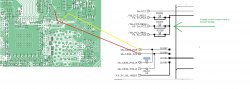
I will give examples of problems that are often encountered from ps3, especially on the RSX CXD2971, I took pictures from the DIA-001
view

remember !!!, this is just an example, in my picture the pin-pin connection data from CellBe to RSX, a common problem that occurs in the CXD2971, when measuring resistance in IC using a digital meter (fluxe) pin 1 and pin 2 is drawn shot , pin1 and pin2 are connected internally in RSX, which shouldn't happen, that's what causes PS3 YLOD. Then I heat the RSX CXD2971 with a temperature increase of max 200c for 15 minutes, after it cools down I re-measure pin1 and pin2 that were previously connected, the RESULT? pin1 and pin2 separate back to normal, no longer connected, from such conditions I conclude that using heat can change the conditions inside the RSX CXD2971, but such repairs cannot last long, 2-3 days later pin1 and pin2 are shot again, reconnected Internally in RSX, there are a lot of similar cases like this with different results, but from the many ps3s that have been treated like this, I conclude:
1. RSX that has never been HEATED, will last quite a long time, approx. 3-6 months, will have a longer lifespan if it is used frequently, harvested continuously
2. RSX that has been HEATED, DON'T WASTE YOUR TIME, REPLACE RSX CXD530XX IMMEDIATELY !!!!!
That's why my brother("KIAW'S) made the MODRSX IC so that the old CXD2971 could be replaced.
how to heat RSX like this can only be done on RSX CXD2971, does not apply to other RSX, why? Ask Sony ...(what is clear is that the make is different)
BUT if you don't have a problem doing that, it's okay too, in principle heating to 2,3,4,5 makes the PS3's life time less and less, it's good that it doesn't interfere with other components, until it's time you replace the RSX ...
other than heating (CXD2971 only), repairing ps3 that enters "rules3" is by:
1. Replace tin ore, reballing either RSX or Cellbe, just one of them
2. Replace RSX or Cellbe because it is damaged

It seems that I also explain it for a long time, I leave it up here, hopefully it will be useful and keep up the spirit, as usual, no method is perfect, take the important parts, combine it with other methods, make it more perfect, that too is my hope , I am 47 years old, my ability to service has decreased, my eyes are also myopic, I like your enthusiasm in finding and learning something new, I hope that in the future you can produce more perfect methods I pray everyone will be well always (

@botakompong, I tried to follow this post as best I could but I had a few problems when trying to decipher your method:
  • Where exactly are the testpoints? Eg. C1, C2, C3, C4, and R1, R2, R3, R4, R5? I couldn't tell from your pictures exactly where each point is. Could you use a COK-001 or COK-002 board for the example? We have schematics for them, so it'll make it easier for me to figure out which voltage you're referring to (Eg. VDDA or VDDIO, that kind of thing). Or you could save me time by just saying C1 = VDDC, C2 = VDDR, etc.
  • When you showed video of the voltage kicks, you didn't show which test point you are probing on camera. You said you were alternating between them, but if you were starting with C1, then C2, then C3, then C4, then back to C1, the second time you get to C1 doesn't match the first kick? So you must have done one of them twice and I can't tell which test is C1 or C2? So it's impossible to follow. You gotta show us where you're probing, or do separate short videos for each test point.
Thanks for posting your method, it's interesting and no doubt useful. We just need to be able to follow it...lol!
 
SB pins for sem001 if they are added dont know,jut to confirm proof of miising parts
You mean they physically disabled the SB UART by not placing 0k resistors on the RX/TX lines? So you would have to short those pads to enable it?

That's a common way of disabling UART or JTAG ports form the factory before commercial release. They just leave components off the board. It reduces the BOM too. So from an engineering perspective that makes sense.
No short missing resistance is to enable traces up to unpopulated CN-ports on boards. Kindly opțional.
SB and SC rxtx can still be used for normal users where already factory left alloy soldered.
Apart from this still many undocumented parts are left, only listed partially parts are in sem001 schematic pdf.
 
No short missing resistance is to enable traces up to unpopulated CN-ports on boards. Kindly opțional.
SB and SC rxtx can still be used for normal users where already factory left alloy soldered.
Isn't that what I said? Even if you were to solder a port in place, it wouldn't work unless you enabled it by populating those resistors (which are just jumpers). And without a schematic, you wouldn't know to do that.

This is how they increase "security" (stifle reverse engineering, which is perfectly legal).
 
I added these pictures to my tutorial. Thanks for them! I did not add the chart at the end, I felt it is a bit to advanced for a beginner's tutorial. However, I could add a more advanced section, but someone will need to compile a list of commands that generates the info we think would be useful to have. For example, what command generates the above information?
I know what you mean, the chart is fine and all that, but it would be a lot more intuitive if you compare it with this image, is the syscon EEPROM map (virtual, but matches with the kind of access we have by UART)
wN85nx4.png

Let me post the chart again to compare them
a9pfdoR.jpg

"Cookie old" are the COK-001 and COK-002 only... and "cookie new" all the other motherboards with a mullion syscon (BGA 200 balls)
The EEPROM map of the sherwood syscons (with pins all around) doesnt appears in that image

The region names shown in the chart seems to be official codenames from that image
The column with the "checksum at address" for mullions is printed by the "eepcsum" command in mullions... and for sherwoods that address was found by @Pacorretaco (because the "eepcsum" command doesnt prints that info in sherwoods he had to search in the dump)
The "regions covered" for mullions was found by m4j0r and friends (with the help of a python script published by m4j0r used to calculate that checksums in PC)
And the "regions covered" for sherwoods was found by me, using the PC python script from m4j0r and the address mentioned by pacorretaco, i just had to find where it starts

Long story short... if you write something in that regions protected by a checksum the next thing that is going to happen is when you run the "eepcsum" command syscon is going to complain that there are checksums that needs to be fixed (and syscon is going to tell you the value you need to write for the new checksum)
So.. you can take a look at the chart to see the name of the region with a broken checksum, and the address where you need to write the new checksum

Is pretty much the same info given by the "eepcsum" command but with more details
 
Last edited:
In the beginning with time I will practice first and report via pm all tests. Not putting on public in first place, don't want to be responsible for mistakes.
At one point I may get some syscon flash models for experimental tests.
Also left layer 7 to be scrambled and test few I should find it easy. Now best tool used to find quick then schematic (to be used only on scrap boards, not to good one) :)
50b8c87c8c5f87bca6cbf9e66bc71160.jpg
Edit
About my shitty dyn001 board will stay forever with this error. Cpu thermal diode inside looks good compared with work boar (checked all parts with cap/without,took, signal from rsx d+, D- to his imput. )

This have to be sorted faster, if I work more than 2 days on a board I rather leave it for parts.
Atm ported another syscon and need to flash nor, left cpu to be reballed (another set from working board. If this will give same error I just going by hammer.
 
Last edited:
@botakompong, I tried to follow this post as best I could but I had a few problems when trying to decipher your method:
  • Where exactly are the testpoints? Eg. C1, C2, C3, C4, and R1, R2, R3, R4, R5? I couldn't tell from your pictures exactly where each point is. Could you use a COK-001 or COK-002 board for the example? We have schematics for them, so it'll make it easier for me to figure out which voltage you're referring to (Eg. VDDA or VDDIO, that kind of thing). Or you could save me time by just saying C1 = VDDC, C2 = VDDR, etc.
  • When you showed video of the voltage kicks, you didn't show which test point you are probing on camera. You said you were alternating between them, but if you were starting with C1, then C2, then C3, then C4, then back to C1, the second time you get to C1 doesn't match the first kick? So you must have done one of them twice and I can't tell which test is C1 or C2? So it's impossible to follow. You gotta show us where you're probing, or do separate short videos for each test point.
Thanks for posting your method, it's interesting and no doubt useful. We just need to be able to follow it...lol!
Ok friends, later I will take a photo of the measurement area from C1,C2,C3,C4 and R1,R2,R3,R4,R5, I did separate the video specifically for C1 and R1. For C2, C3, C4 videos, I did combine them into 1 video, where the measurements of each area took turns, from C2 to C3 to C4 then back again to C2 to C3 to C4 and so on, as well as R2, R3, R4, R5 I combined the measurements into 1 video like C2, C3, C4.
Video C1 / R1 represents a voltage that has no kick
Video (C2,C3,C4) / (R2,R3,R4,R5) represents a voltage that has a kick

Forgive me for still using handwriting, using a program to show something takes a long time for me, here are my photos, hope it's clear. in my rsx ic just number 1,2,3,4,5 which represents R1,R2,R3,R4,R5
IMG_20210616_105523.jpg
IMG_20210616_103807.jpg
IMG_20210616_103322.jpg
IMG_20210616_104108.jpg
there is a point in the area in my mark because it does not include the voltage area
IMG_20210616_103857.jpg
IMG_20210616_104034.jpg
IMG_20210616_103905.jpg
IMG_20210616_104640.jpg
IMG_20210616_112322.jpg
IMG_20210616_112445.jpg
Sorry if the picture is bad...from COK-001
 
Last edited:
@botakompong's Pulse CLK method of troubleshooting PS3's.
The video above shows how a normal "Pulse CLK" behaves. Note, you need an analog volt meter to follow this method. Alternatively you could use an Oscilloscope with a time scale set to record around 20s worth of data. When you watch the video notice that the first pulse raises the voltage. That's the "first Kick." About 2s in, it fluctuates and raises a bit more, at around the 5-6s mark in the video. That's the "second Kick." And just before the video appears on screen the "third kick" occurs. The whole process takes about 20s.

Below I have re-written @botakompong's previous posts into one place. It shows what's happening during each "Kick" and how a console with each type of fault will look. Hopefully this makes it easier to follow his method of troubleshooting/diagnosing consoles.

"Pulse CLK" Testpoint Locations:
Pulse CLK COK-001.jpg
Pulse CLK COK-002.jpg
Pulse CLK SEM-001.jpg
Pulse CLK DIA-001&2.jpg
Pulse CLK All Slim.jpg
Pulse CLK All Super Slim.jpg

Kick 1 = After PWR ON the voltage should kick up and stay there. During this time, Bootup Sequences 1-5 occur.
Symptoms: YLOD
  • Pulse CLK fails Kick 1. Rises to 1.5v or less and drops back to 0v followed by an instant YLOD (>1s).
  • 1x beep after pressing reset.
Possible Cause:
  • Incorrect CPU input voltage (4 of them)
    • C1 = 1.2v VDDC. No kick pwr. Pulse CLK will not kick = Instant YLOD (<1s).
      • If that's the case, then check resistors around IC6103 with a known good board and replace any bad ones.
      • Damaged NEC/TOKINs cause noisy PWR. Tokins can cause a YLOD that, in order of most to least common, occurs only in intense games, normal stress, delayed 10s – 5 mins, and non-instant (3 - 7s). The SYSCON code will be a 1002. However, if severely damaged they can cause a cause an instant YLOD (<1s) with a 3004 SYSCON error. But that is rare!
    • C2 = 1.2v_YC_RC_VDDIO
    • C3 = 1.2v_YC_RC_VDDIO
    • C4 = 1.5v_YC_RC_VDDA
  • CPU BGA defect
  • Damaged CPU
Symptoms: YLOD
  • Pulse CLK fails Kick 1. Rises to only 1.5v and drops back to 0v followed by an instant YLOD (<1s).
  • 1x beep after pressing reset.
Possible Cause:
  • Incorrect RSX input voltage (5 of them)
    • R1 = 1.3v VDDC. No kick pwr. Pulse CLK will not kick = Instant YLOD (<1s).
      • For 90nm and 65nm RSX: If that's the case, then NEC/TOKINs are the issue. Damaged NEC/TOKINs cause noisy PWR. Tokins can cause a YLOD that, in order of most to least common, occurs only in intense games, normal stress, delayed 10s – 5 mins, and non-instant (3 - 7s). The SYSCON code will be a 1002. However, if severely damaged they can cause a cause an instant YLOD (<1s) with a 3004 SYSCON error. But that is rare!
      • If not above or for 40nm and 28nm RSX: Check resistors around IC6201 with a known good board and replace any bad ones.
    • R2 = 1.2v VDDR
    • R3 = 1.5v_VDDA
    • R4 = 1.5v_VDDIO
    • R5 = 1.8v_VDDQ
  • CPU BGA defect
  • Damaged CPU
Symptoms: YLOD
  • Pulse CLK goes high and stalls. It does not fluctuate. Does not enter kick 2. Or it goes high and falls back down. Both cases cause YLOD.
  • 1x beep after pressing reset.
  • No bad CPU or RSX voltages.
  • 3034 and associated 40xx SYSCON error. Use a bringup command to start the console and log the startup sequence. It's possible to get "RSX: Bit training error" or "BE: Bit training error."
Possible Cause:
  • BGA (most likely) or Die Bumps (less likely) on either the CPU (less likely) or RSX (most Likely).
  • Damaged FlexIO traces between CPU-RSX.
  • Manufacturing defect, or corrosion from poor environment.
  • Shorting RSX and/or CPU internal pins (electromigration). Accumulated heat damage that cannot be repaired. It can be temporarily revived by heating, but it will not last. It needs replaced.
  • The usual repair attempts (in order) are to reball the RSX. If that does not work, then reball the CPU. If neither work, then replace the RSX (same model) with a working chip. Beyond that it is too difficult to continue. The console is dead.
Symptoms: GLOD
  • Pulse CLK passes Kick 1. Attempts kick 2 but fails and retries in an endless loop.
  • No display / Black screen.
  • No beep after pressing reset.
  • HDD LED not blinking. No HDD access.
Possible Cause:
  • Incorrect CPU_RAM input voltage (2 of them)
  • CPU BGA defect
  • Damaged CPU or RAM
Example Video:
Symptoms: YLOD
  • Pulse CLK passes Kick 1. Attempts kick 2 but fails and falls way back, kicks up again and fails. Falls back to zero and stays there.
  • 1x beep after pressing reset.
Possible Cause:
  • Corrupted OS
  • Incorrect FW, such as a bad softmod.

Kick 2
= is quicker and smaller, but noticeable. During this time, Bootup Sequence 6 occurs
Symptoms: GLOD
  • Pulse CLK passes kick 1. Kick 2 is weak and stalls. No looping.
  • No display / Black screen.
  • 1 beep after pressing reset.
  • HDD LED blinks briefly, ruling out a problem in #4.
Possible Cause:
  • Incorrect RSX_RAM input voltage
  • RSX BGA defect
  • Damaged RSX or RAM

Kick 3
= is weak. During this time, Bootup Sequence 7 occurs.
Symptoms: GLOD
  • Pulse CLK looks normal.
  • No display / Black screen.
Possible Cause:
  • Damaged HDMI or AV port
  • Damaged HDMI encoder (IC2502)
  • Damaged AV Driver (IC2406)
  • Perhaps check the ESR of the electrolytic by the AV Driver chip.

RSX Chips:

CXD2971x = Kick 1 & 2 only before image appears
CXD2982x, 2991x, 530xx = Have all 3 kicks.

YLOD Causes: A problem with any of the following will cause a YLOD
1. Cell BE Issue
2. RSX Issue
3. RSX<-->CELL isssue not related to voltages or BGA Defects.
4. BootOS Issue​

GLOD Causes: A problem with any of the following will cause a GLOD
1. CPU RAM Issues
2. RSX RAM Issues
3. AV / HDMI Issues
4. OS Software Issues
5. HDD ISsues
 
Last edited:
Ok friends, later I will take a photo of the measurement area from C1,C2,C3,C4 and R1,R2,R3,R4,R5, I did separate the video specifically for C1 and R1. For C2, C3, C4 videos, I did combine them into 1 video, where the measurements of each area took turns, from C2 to C3 to C4 then back again to C2 to C3 to C4 and so on, as well as R2, R3, R4, R5 I combined the measurements into 1 video like C2, C3, C4.
Video C1 / R1 represents a voltage that has no kick
Video (C2,C3,C4) / (R2,R3,R4,R5) represents a voltage that has a kick

Forgive me for still using handwriting, using a program to show something takes a long time for me, here are my photos, hope it's clear. in my rsx ic just number 1,2,3,4,5 which represents R1,R2,R3,R4,R5
View attachment 33759
View attachment 33757
View attachment 33758
View attachment 33760
there is a point in the area in my mark because it does not include the voltage area
View attachment 33762
View attachment 33763
View attachment 33764
View attachment 33765
View attachment 33766
View attachment 33767
Sorry if the picture is bad...from COK-001
Thanks for that. Please have a look at my above post and let me know if I got all that right! It took most of the day to figure out...lol! I'd like to add to it if we can make the method better or you find anything I should add to it.

For example, where exactly is the "Pulse CLK" test point? Or is it C1-4 and R1-5?
 
In the beginning with time I will practice first and report via pm all tests. Not putting on public in first place, don't want to be responsible for mistakes.
At one point I may get some syscon flash models for experimental tests.
Also left layer 7 to be scrambled and test few I should find it easy. Now best tool used to find quick then schematic (to be used only on scrap boards, not to good one) :)
50b8c87c8c5f87bca6cbf9e66bc71160.jpg
Edit
About my shitty dyn001 board will stay forever with this error. Cpu thermal diode inside looks good compared with work boar (checked all parts with cap/without,took, signal from rsx d+, D- to his imput. )

This have to be sorted faster, if I work more than 2 days on a board I rather leave it for parts.
Atm ported another syscon and need to flash nor, left cpu to be reballed (another set from working board. If this will give same error I just going by hammer.
Aha, now that looks like a pro hacker tool!

About your DYN 001 with funny thermal sensor...
This may sound silly, but it occurs to me, what if you modify the syscon to disable the safety thermal shutdown?
It's dodgy but if you are having thermal shudtdown while the temperatures are actually under control... Maybe you could try to fool the syscon if you don't know what else to do?
I think even in sherwood you can still make temporary changes to volatile Syscon RAM. Just for test without messing with checksum. The changes will disappear automatically next time the standby power is lost. So really no danger in trying.

tshutdown set 0 255
tshutdown set 1 255

Although... Yeah you say your 1200 error is gone already... So probably the problem is something else?
Oh well
 
@botakompong's Pulse CLK method of troubleshooting PS3's.

Pulse CLK:

Kick 1
= After PWR ON the voltage should kick up and stay there. During this time, Bootup Sequences 1-5 occur.
Symptoms: YLOD
  • Pulse CLK fails Kick 1. Rises to 1.5v or less and drops back to 0v followed by an instant YLOD (>1s).
  • 1x beep after pressing reset.
Possible Cause:
  • Incorrect CPU input voltage (4 of them)
    • C1 = 1.2v VDDC. No kick pwr. Pulse CLK will not kick = Instant YLOD (<1s).
      • If that's the case, then check resistors around IC6103 with a known good board and replace any bad ones.
      • Damaged NEC/TOKINs cause noisy PWR. Tokins can cause a YLOD that, in order of most to least common, occurs only in intense games, normal stress, delayed 10s – 5 mins, and non-instant (3 - 7s). The SYSCON code will be a 1002. However, if severely damaged they can cause a cause an instant YLOD (<1s) with a 3004 SYSCON error. But that is rare!
    • C2 = 1.2v_YC_RC_VDDIO
    • C3 = 1.2v_YC_RC_VDDIO
    • C4 = 1.5v_YC_RC_VDDA
  • CPU BGA defect
  • Damaged CPU
Symptoms: YLOD
  • Pulse CLK fails Kick 1. Rises to only 1.5v and drops back to 0v followed by an instant YLOD (<1s).
  • 1x beep after pressing reset.
Possible Cause:
  • Incorrect RSX input voltage (5 of them)
    • R1 = 1.3v VDDC. No kick pwr. Pulse CLK will not kick = Instant YLOD (<1s).
      • For 90nm and 65nm RSX: If that's the case, then NEC/TOKINs are the issue. Damaged NEC/TOKINs cause noisy PWR. Tokins can cause a YLOD that, in order of most to least common, occurs only in intense games, normal stress, delayed 10s – 5 mins, and non-instant (3 - 7s). The SYSCON code will be a 1002. However, if severely damaged they can cause a cause an instant YLOD (<1s) with a 3004 SYSCON error. But that is rare!
      • If not above or for 40nm and 28nm RSX: Check resistors around IC6201 with a known good board and replace any bad ones.
    • R2 = 1.2v VDDR
    • R3 = 1.5v_VDDA
    • R4 = 1.5v_VDDIO
    • R5 = 1.8v_VDDQ
  • CPU BGA defect
  • Damaged CPU
Symptoms: YLOD
  • Pulse CLK goes high and stalls. It does not fluctuate. Does not enter kick 2. Or it goes high and falls back down. Neither case causes YLOD.
  • 1x beep after pressing reset.
  • No bad CPU or RSX voltages.
  • 3034 and associated 40xx SYSCON error. Use a bringup command to start the console and log the startup sequence. If you get a "RSX: Bit training error" then it's a RSX issue.
Possible Cause:
  • Damaged traces between CPU-RSX.
  • Manufacturing defect or corrosion from poor environment.
  • Shorting RSX internal pins (electromigration). Accumulated heat damage that cannot be repaird. Can be temporarily revived by heating, but it will not last. It needs replaced.
Symptoms: GLOD
  • Pulse CLK passes Kick 1. Attempts kick 2 but fails and retries in an endless loop.
  • No display / Black screen.
  • No beep after pressing reset.
  • HDD LED not blinking. No HDD access.
Possible Cause:
  • Incorrect CPU_RAM input voltage (2 of them)
  • CPU BGA defect
  • Damaged CPU or RAM
Symptoms: YLOD
  • Pulse CLK passes Kick 1. Attempts kick 2 but fails and falls way back, kicks up again and fails. Falls back to zero and stays there.
  • 1x beep after pressing reset.
Possible Cause:
  • Corrupted OS
  • Incorrect FW, such as a bad softmod.
Kick 2 = is quicker and smaller, but noticeable. During this time, Bootup Sequence 6 occurs
Symptoms: GLOD
  • Pulse CLK passes kick 1. Kick 2 is weak and stalls. No looping.
  • No display / Black screen.
  • 1 beep after pressing reset.
  • HDD LED blinks briefly, ruling out a problem in #4.
Possible Cause:
  • Incorrect RSX_RAM input voltage
  • RSX BGA defect
  • Damaged RSX or RAM
Kick 3 = is weak. During this time, Bootup Sequence 7 occurs.
Symptoms: GLOD
  • Pulse CLK looks normal.
  • No display / Black screen.
Possible Cause:
  • Damaged HDMI or AV port
  • Damaged HDMI encoder (IC2502)
  • Damaged AV Driver (IC2406)
  • Perhaps check the ESR of the electrolytic by the AV Driver chip.

RSX Chips:

CXD2971x = Kick 1 & 2 only before image appears
CXD2982x, 2991x, 530xx = Have all 3 kicks.

YLOD RULES: A problem with any of the following will cause a YLOD
1. Cell BE Issue
2. RSX Issue
3. RSX<-->CELL isssue not related to voltages or BGA Defects.
4. BootOS Issue​

GLOD RULES:
1. CPU RAM Issues
2. RSX RAM Issues
3. AV / HDMI Issues​
later I will take a photo of the clk point for all types of ps3, I am very impressed that you can capture and describe it well, just like reading an electronic book...lol btw tq alot..
My english is not good, maybe i have to read it many times so i can understand
 
Last edited:
@victor, it seems I made a mistake in the analysis, error 2024 and error 2124, it is a damage in cellbe connection area with rsx or connection area with sub cxd9963 (final rule3), not related to CellBe RAM, I have corrected the damage by replacing 1 set cellbe, now the ps3 is normal, unfortunately I didn't record the clk pulse, it's rare to find a ps3 with such damage. Now I can say RAM Rsx and Ram Cellbe are not included in the syscon error.
Someone can correct me if i'm wrong
 

Similar threads

Back
Top