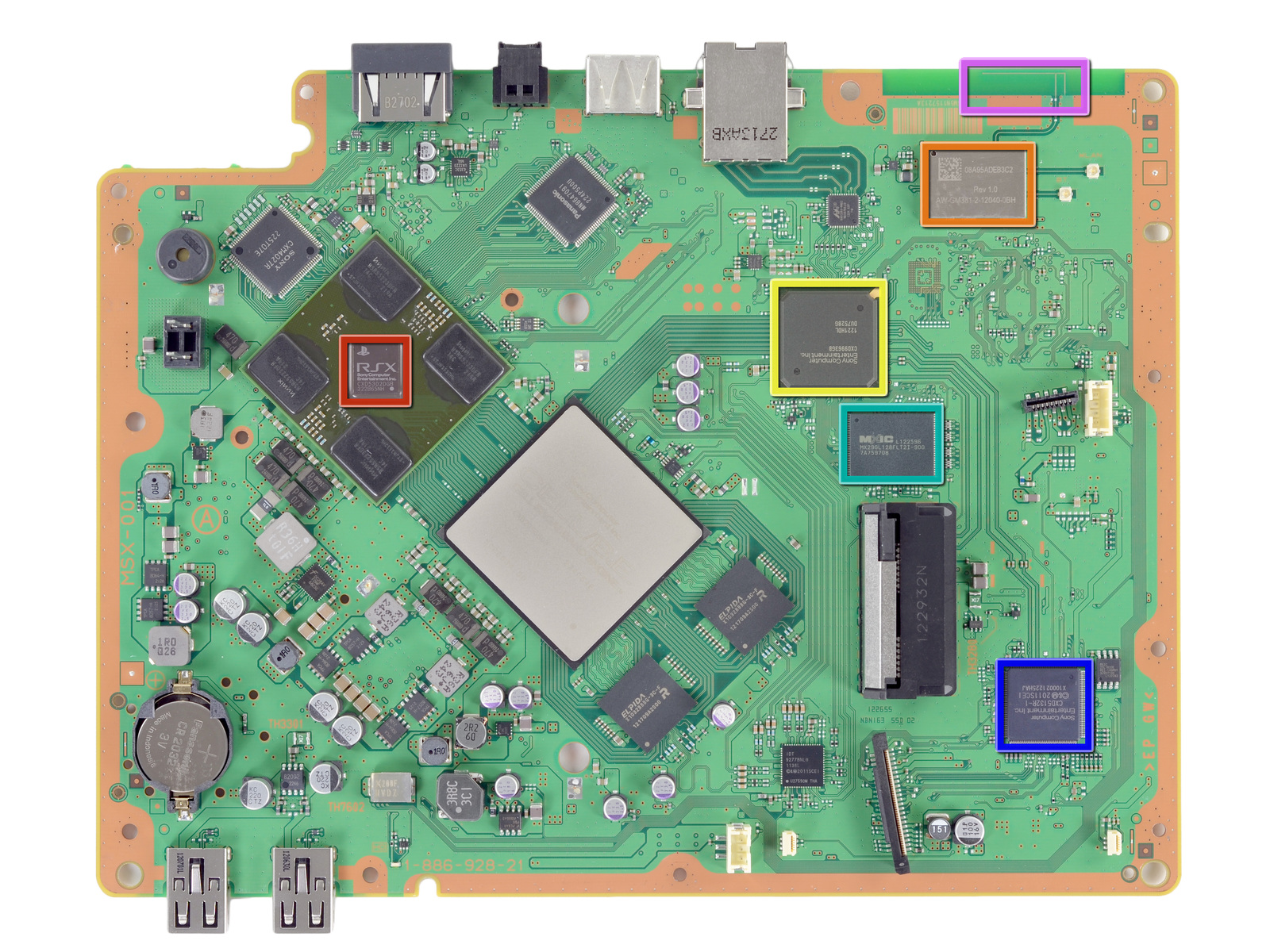
@vyktormvmpay25 is correct, pages 5, 9, and 13 of the COK-001 schematic detail the pinout of the CPU, RSX, and Southbridge respectively. Someone has painstakingly entered the data for the CELL BE, but not the RSX or southbridge yet. It's the more accurate way to do this however.
I see, i cant get the compromise to update all that pad layouts, we are talking around 1500+ pads each but eventually i will keep an eye at the info published and will try it a bit, im busy with other playstation adventures latelly and i would like to do another different things in wiki that i had in my "to do" list since many time ago
What i can do is the same i did with the RSX pad layouts, i mean... is needed to create a template for CELL, and display that template in all the pages of the components that uses the same exact layout
Btw, the CELL pages where appears his pad layouts have a problem, if you click in "edit" in them you are going to realize is duplicated, and thats very bad, because if someone edits one of the pages the other page is going to be outdated
https://www.psdevwiki.com/ps3/CXD2964GB
https://www.psdevwiki.com/ps3/CXD2964AGB
So... i need to do the same trick, a single template for this specific pad layout... but before "merging" them i need to compare them to see if someone edited one of them (but forgot to edit the other)
Also, im going to have the same problem when i was doing the pad layout templates for the RSX... the point is... i need to give them a name, and it should be explicit, and the better way to figure an intuitive name is to know in how many CELL models uses that pad layout
In other words... if we take the complete CELL familly including all the CELL models... how many pad layout templates we have ?, someone knows and can do a resume to help me take this decission about how to name them ?
@sandungas, I'm used to looking at the board view on page 29 of the COK-001 schematic, which has the board orientated with the tokins above the CPU/GPU. I misspoke about the wiki motherboard pics, they indeed have it upside down! I now remember I had to flip the image before making the flowchart.
But dont focus your attention only in the texts printed/etched in the COK-001 motherboard and the service manuals, the RSX pad layout we are discussing is used in lot of PS3 motherboards:
-All retail fats
-All retail slims
-All retail superslims... (except the latests REX-001 and i guess RTX-001 or so with a 28nm RSX)
-All reference tool models (DECR-100 and DECR-1400)
-Probably all the
prototypes and non-retail PS3 models
This pad layout is so generic that we should not use as reference the motherboard name printed in it (e.g. the rotation of the name COK-001 doesnt matters)
And the rotation of this motherboard names is not dependant of the rotation of the CELL/RSX/SB/EEGS texts etched in the IHS
The service manual doesnt shows the texts etched in the metal, you need to imagine them to understand what im going to say, if you take a look at the service manual of the COK-001 and you compare it with a real photo you are going to realize all the names etched in the IHS's are inverted
Also, note the location of pad A1 in the image of the service manual in CELL/RSX/SB/EEGS is different, CELL and RSX have pad A1 at north-west corner, but SB and EEGS at north-east corner... but for some magical reason (aesthetics) all the texts in the IHS's are aligned with each others, because this way you can read all them from the same perspective view
In other words... they are rotating the texts etched in the IHS's just for readability reasons, but that rotation is not related with the location of pad A1
I still recommend you keep the same orientation with the RSX as the CELL BE is documented in the Wiki.
I know, this problem with rotations is taken to many other wiki pages, but thats because the PS3 scene started soon in the PS3 lifetime and everybody was documenting stuff from the COK-001, also the only service manuals leaked are for COK-001, COK,002, SEM-001 as far i know so people had a bigger tendence to follow whatever rotation rules sony used in COK-001
But dont worry, the rotation of the custom images doesnt changes the pad names, when i realized about that i was a bit "feeeew so the pad info in wiki is fine and the image made by Kiaw matches"
The only disagreement is the rotations and how confusing or intuitive could be to represent the custom images with different rotations, and i think the reason why i have a different oppinion is because im thinking in all the PS3 models, included superslims
In few words... in my oppinion the most intuitive way is to ignore the rotation of the motherboard names and ignore also the rotation of the names etched in the IHS because both are misleading
The other day i said that we should not use any other reference than the pad A1 marks that appears in the motherboard (and the IHS... or at a corner of the substrate in the superslims RSX models without IHS)
But later i realized there is a detail from the circuit design that can be used for reference, in this image RSX is at north and CELL at south
The data bus in between then is the in/famous FlexIO, related with the bittraining errors
This design is common for all the PS3 models because the bus needs to be very short and are pretty much straight lines
Note the texts rows for the pad names with A,B,C,D,E,F are aligned with each other and im rotating the image to make them readable (rotated in the same way than the texts when you are reading a book)
Now... what im going to say is just theoretical because sony never did it
Lets say... if they wanted to align the texts CELL and RSX with the pad names they would have made this
But they never did it because the rotation of the texts CELL/RSX is not derivated from the pad names, in this case what they did is to rotate the texts 90º in clockwise direction, this way
See how well it fits if we compare it with the photo of a PS3 slim motherboard taken from a perspective with the HDMI connector at north
https://www.psdevwiki.com/ps3/images/a/a0/JSD-001_(top_view).jpg
And for the superslims doesnt makes sense to use the rotation of the texts CELL/RSX as a reference for the pad layout because the RSX doesnt have a IHS and are in diagonal
The RSX text is rotated 45º in clockwise direction
The CELL text is rotated 90º in clockwise direction


")